Shalow groove isolation manufacturing method for preventign acute angle

A manufacturing method and shallow trench technology, which can be used in semiconductor/solid-state device manufacturing, electrical components, circuits, etc., and can solve problems such as complicated manufacturing processes

Inactive Publication Date: 2005-08-31
MACRONIX INT CO LTD
View PDF1 Cites 0 Cited by
  • Summary
  • Abstract
  • Description
  • Claims
  • Application Information

AI Technical Summary

Problems solved by technology

Chatterjee et al. use the LOCOS method to form a bird’s beak (bird’sbeak) structure to avoid the sharp angle effect, but the manufacturing process is very complicated (IEEE, 1996)

Method used


Image

  • Shalow groove isolation manufacturing method for preventign acute angle
  • Shalow groove isolation manufacturing method for preventign acute angle
  • Shalow groove isolation manufacturing method for preventign acute angle

Examples


Embodiment Construction

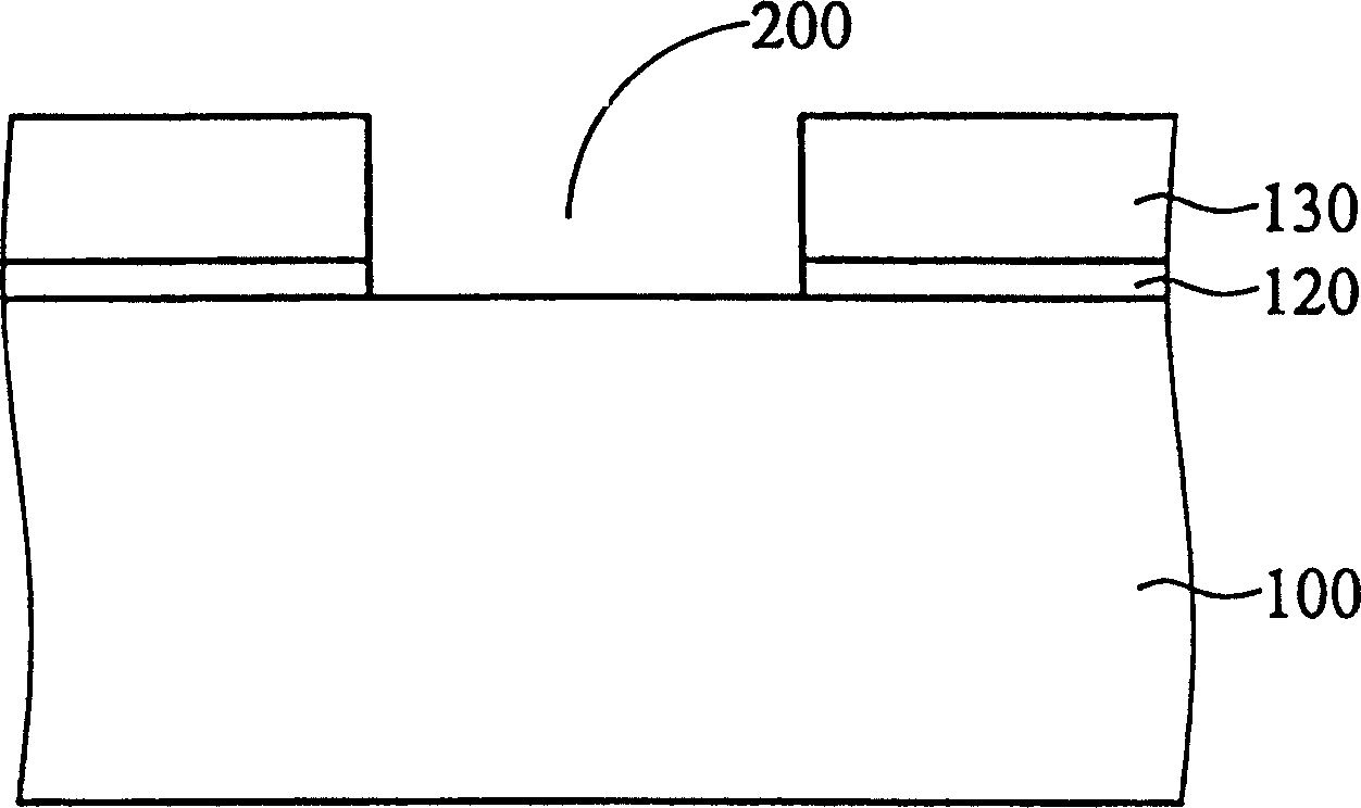
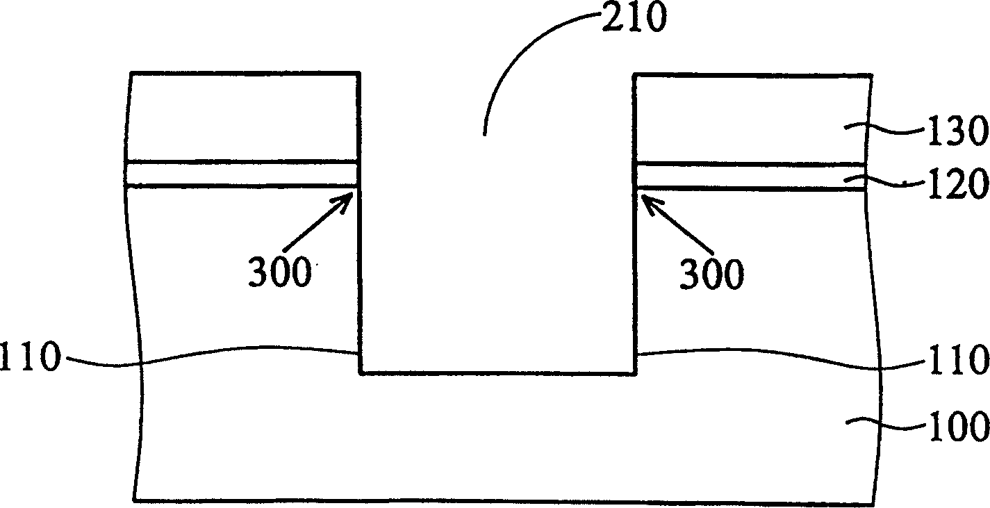
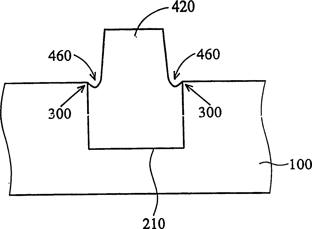
[0047] Figures 2a to 2e A schematic cross-sectional view of a manufacturing method for manufacturing a shallow trench (STI) structure that avoids sharp angles according to a preferred embodiment of the present invention.

[0048] see Figure 2a A silicon oxynitride (SiON; silicon oxynitride) layer 12 and a masking layer 13 are sequentially formed on a semiconductor substrate 10 . The semiconductor substrate is, for example, a silicon substrate. The formation method of SiON layer 12 is: for example, using SiH 4 , N 2 O, N 2 The reaction gas is formed by low pressure chemical vapor deposition (LPCVD; low pressure chemical vapor deposition) or plasma-assisted chemical vapor deposition (PECVD; plasma-enhanced chemical vapor deposition), and the thickness can be between 150 Å and 250 Å. The shielding layer 13 can be a silicon nitride layer, and dichlorosilane (SiCl 2 h 2 , dichlorosilane) and NH3 are reactive gases, formed by LPCVD, and the thickness can be between 1500 Å a...


PUM


Abstract

A process for preparing the shallow channel isolation without sharp angle includes sequentially generating SiON layer and masking layer on a semiconductor substrate, defining them to form a window to expose the substrate, generating spacer on the side wall of SiON layer and masking layer, generating a shllow channel on the semiconductor substrate, generating a lining oxide layer on the surface of shallow channel to form a beak-shaped lining oxide layer near the SiON layer, filling the isolation oxide layer in channel, and removing the masking layer and SiON layer. Its advantages are high thickness uniformity of oxide layer tunnel, and no parasitic transistor and electric leakage.

Description

technical field [0001] The invention relates to a shallow trench isolation manufacturing method, in particular to a shallow trench isolation manufacturing method avoiding acute angles. Background technique [0002] With the development of semiconductor manufacturing technology to submicron size, shallow trench isolation (STI; shallow trench isolation) has gradually replaced traditional semiconductor device isolation methods, such as local oxidation of silicon (LOCOS; local oxidation of silicon). Compared with LOCOS, STI has many advantages. For example, the STI method can make the semiconductor device isolation structure have a smaller width and thus have a higher device density. In addition, STI can improve the surface flatness, so it can effectively control the minimum line width (critical dimension) during lithography. [0003] Figures 1a to 1c It is a schematic cross-sectional view of a manufacturing method for manufacturing an STI structure according to a conventional...

Claims


Application Information

Patent Timeline
Patent Type & Authority Patents(China)
IPC IPC(8): H01L21/76H01L21/762
CPCH01L21/76235
Inventor 蔡文彬吴俊沛陈辉煌
Owner MACRONIX INT CO LTD
Why Eureka
Try Eureka