
Light-emitting semiconductor device capable of being surface mounted and with composite packing structure

A light-emitting semiconductor and flip-chip packaging technology, which is applied in the direction of semiconductor devices, electrical solid devices, electrical components, etc., can solve problems such as unfavorable size miniaturization, and achieve the effects of simplification of subsequent steps, high light output efficiency, and material stress reduction

Inactive Publication Date: 2005-02-16
EPISKY
View PDF0 Cites 0 Cited by
  • Summary
  • Abstract
  • Description
  • Claims
  • Application Information

AI Technical Summary

Problems solved by technology

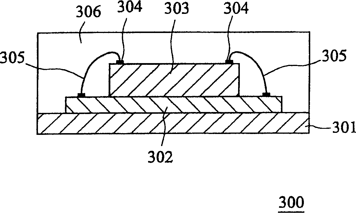
[0006] It can be seen from the packaging structure of the above-mentioned traditional light-emitting diode device that whether it is a wire-type or a chip-type packaging structure, it needs to go through packaging steps such as wire bonding; moreover, the packaging method of the traditional wire-type light-emitting diode device is not conducive to its miniaturization. Therefore, it is necessary to propose a packaging structure that can reduce manufacturing costs and packaging performance for the packaging steps of traditional light-emitting diode devices, so as to meet the ever-changing needs of the industry

Method used


Image

  • Light-emitting semiconductor device capable of being surface mounted and with composite packing structure
  • Light-emitting semiconductor device capable of being surface mounted and with composite packing structure
  • Light-emitting semiconductor device capable of being surface mounted and with composite packing structure

Examples


Embodiment Construction

[0056] Figure 4 It is a cross-sectional view showing a light-emitting semiconductor device capable of surface-mounting and having a flip-chip package structure in a preferred embodiment of the present invention.

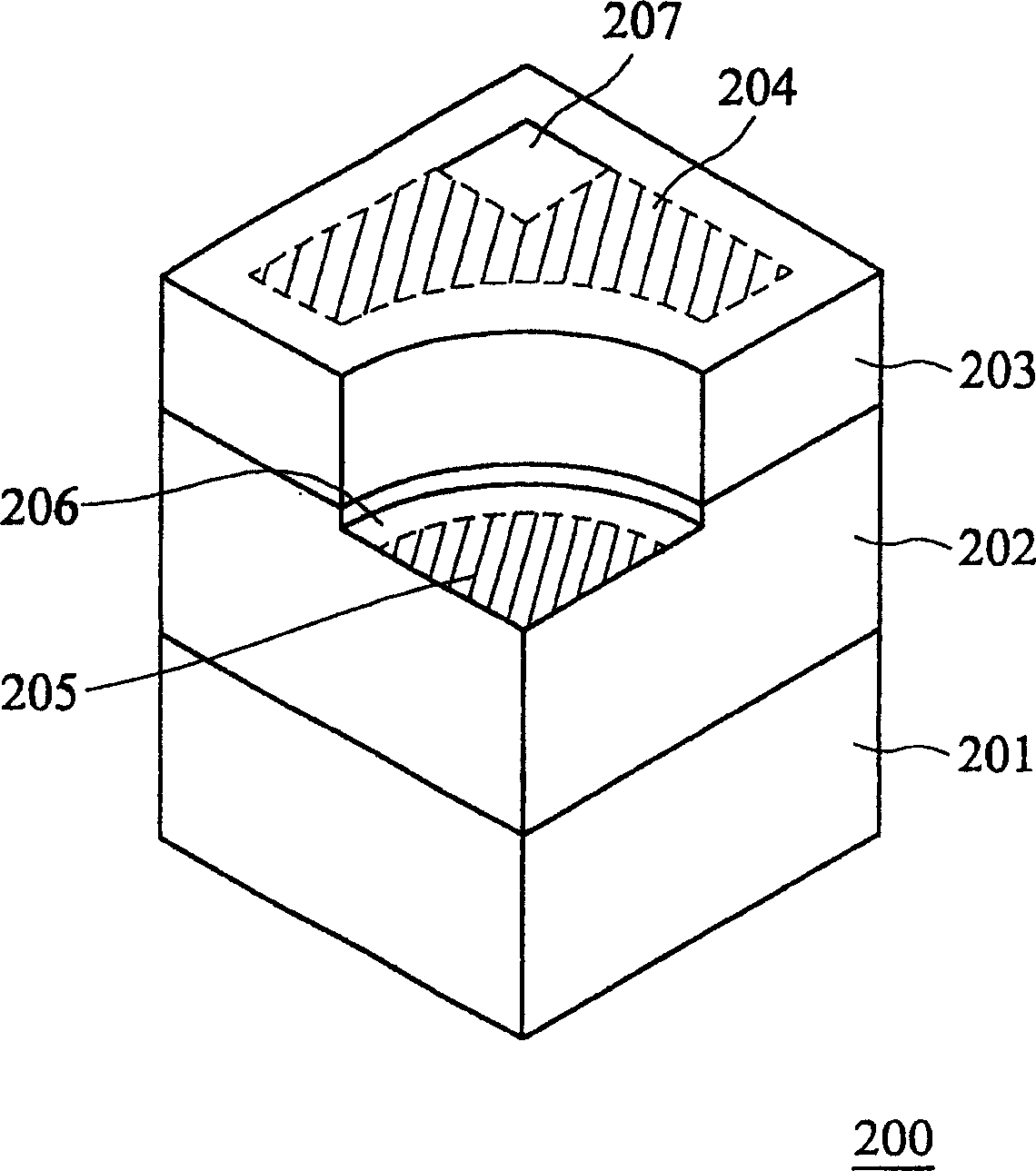
[0057] Such as Figure 4 As shown, according to a preferred embodiment of the present invention, a light-emitting semiconductor device 400 that can be surface-mounted and has a flip-chip package structure includes an insulating substrate 401 and a light-emitting diode 402 . Wherein, the insulating substrate 401 is a ceramic substrate. LED 402 is similar to figure 2The light emitting diode 200, which includes a sapphire substrate 403, an N-type gallium nitride semiconductor layer 404 deposited on the sapphire substrate 403, an active layer 405 deposited on the N-type gallium nitride semiconductor layer 404, and an active layer 405 deposited on the active layer 405 P-type gallium nitride semiconductor layer 406 on it. Wherein, the function of the active layer 405...


PUM


Abstract

The light-emitting semiconductor device package includes insulating base board and LED, the LED includes substrate, the first type semiconductor layer with the first electrode area on the substrate, the second type semiconductor layer with the second electrode area on the first type semiconductor layer, the first electrode formed in the first electrode area and the second electrode formed in the second electrode area. The present invention features that the LED is fixed on the insulating base board via composite mode. There are two electrode layers on two sides of the insulating base board for the surface mounting of the LED device.

Description

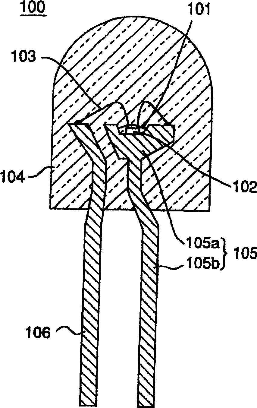
technical field [0001] The invention relates to a light-emitting semiconductor device with a flip-chip packaging structure, in particular to a light-emitting semiconductor device with a flip-chip packaging structure that can be surface-mounted. Background technique [0002] The packaging methods of traditional light-emitting semiconductor devices are nothing more than two types: lead type and chip type. The packaging structure of the wire-type light-emitting semiconductor device is as follows: figure 1 shown in figure 1 Among them, the light emitting semiconductor device 100 includes a light emitting diode 102, a lead holder base 105, and a lead holder side wire 106, wherein the lead holder base 105 is further divided into two parts: a cup-shaped base 105a and a lead holder wire 105b. After installing the LED 102 in the recess of the cup-shaped base 105a, the cup-shaped base 105a is filled with a resin layer 101 such as epoxy resin (epoxy), so that...

Claims


Application Information

Patent Timeline
Patent Type & Authority Patents(China)
IPC IPC(8): H01L33/48H01L33/62
CPCH01L2224/48091H01L2224/48247H01L2224/48257H01L2924/181
Inventor 林明德王冠儒
Owner EPISKY
Learn More