Single-electron memory unit with nano metal oxide wire

A nano-metal, storage unit technology, applied in electrical components, nanotechnology, nanotechnology, etc., can solve the problems of complexity, high operating voltage, and unfavorable stabilization of single-electron memory performance, and achieve simple process and stable operation. Good results

Inactive Publication Date: 2004-09-15
SHANGHAI JIAO TONG UNIV
View PDF0 Cites 0 Cited by
  • Summary
  • Abstract
  • Description
  • Claims
  • Application Information

AI Technical Summary

Problems solved by technology

However, from the perspective of ultra-density integration requiring ultra-low power consumption and ultra-low voltage operation, the operating voltage of this single-electron memory is obviously too high
Moreover, although it is compatible with the classic silicon MOS process, it must be earlier than the production of metallized electrodes in terms of process flow procedures, which will bring disadvantages to the stability of single-electron memory performance, and the production process is relatively ,quite complicated

Method used


Image

  • Single-electron memory unit with nano metal oxide wire
  • Single-electron memory unit with nano metal oxide wire

Examples


Embodiment Construction

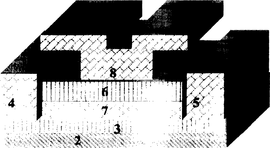
[0011] figure 1 It is a schematic diagram of a three-dimensional structure of an ultra-thin nanometer metal oxide wire TiOx single-electron storage unit according to an embodiment of the present invention.

[0012] Such as figure 1 As shown, the ultra-thin nanometer metal oxide line TiOx single-electron storage unit includes: silicon substrate 2, insulating layer 3 and insulating layer 6, source line 4; data line 5, active area 7 of memory unit, write line 8 . There is a layer of silicon dioxide insulating layer 3 on the silicon substrate 2, an ultra-thin titanium film is deposited on the insulating layer 3, and the active area 7 of the memory cell is locally oxidized, between the active area 7 and the write line 8 of the upper layer Au There is a layer of SiO 2 The insulating layer 6, the source line 4 of Au / Ti and the data line 5 of Au / Ti are located in the active area 7 and SiO 2 both sides of the insulating layer 6. Wherein, the length of the active region 7 is the di...


PUM


Abstract

A milimicron metal oxide line single electron storage unit applies super-thin millimicron metal oxide line as the active region of the single electron storage unit, the thickness is 3nm, the width is one electron local length xi, and the length is 2-5 xi. An SiO2 isolated layer is between the active region and the up-layer writing line, the source line and data line are at both sides of the active region and SiO2 isolating layer, the writing line, data line and the source line are made of Au or Al metal films. Combined with MOSFET millicron, it can realize super-high density IC millicon storage memory of 10 to the power 12 bit, capable of working under room temp. with good stability, competitive with CMOS super large scale IC circuit.

Description

Technical field: [0001] The invention relates to a nanometer metal oxide wire single-electron storage unit, which is used in the technical field of nanometer electronics. Background technique: [0002] Due to the limitation of the principle structure, the traditional silicon MOS memory cannot be single in T Bit (10 12 Bit) play a leading role in ultra-high-density integrated nano-memory. This is because this memory uses a MOS transistor T (often called a gate) controlled by a word line and a capacitor C that stores digital information (0 or 1). S (often called storage capacitance), one of the most important technical indicators of this memory is the charge transfer rate T of the unit Q , in order to ensure correct detection of stored information, T Q Bigger is better, and T Q The size depends on the storage capacitor C S Parallel capacitance C B Ratio, the larger the ratio, the better. C B Limited by the overall design, the minimum is 10 -12 F level. Therefore, onl...

Claims


Application Information

Patent Timeline
Patent Type & Authority Patents(China)
IPC IPC(8): H01L27/10
CPCH01L27/10B82Y10/00
Inventor 蒋建飞蔡琪玉黄萍沈波程子川
Owner SHANGHAI JIAO TONG UNIV
Why Eureka
Try Eureka