Method of epitaxial bipolar device and complementary metallic oxide semiconductor device

A bipolar device and device technology, applied in semiconductor devices, semiconductor/solid-state device manufacturing, electric solid-state devices, etc., can solve problems such as protecting CMOS devices

Inactive Publication Date: 2004-07-14
IBM CORP
View PDF2 Cites 0 Cited by
  • Summary
  • Abstract
  • Description
  • Claims
  • Application Information

AI Technical Summary

Problems solved by technology

The first issue is controlling base outdiffusion during CMOS source / drain (S / D) and lightly doped drain (LDD) annealing
The second issue is how to provide a high-quality epitaxial surface for base growth; the third issue is how to protect the CMOS device during formation of bipolar devices

Method used


Image

  • Method of epitaxial bipolar device and complementary metallic oxide semiconductor device
  • Method of epitaxial bipolar device and complementary metallic oxide semiconductor device
  • Method of epitaxial bipolar device and complementary metallic oxide semiconductor device

Examples


Embodiment Construction

[0024] The present invention providing a method for fabricating a BiCMOS integrated circuit using a gate-last-base processing scheme will be described in more detail below with reference to the accompanying drawings of the present application. It should be noted that in the various figures, like or corresponding parts are denoted by like reference numerals.

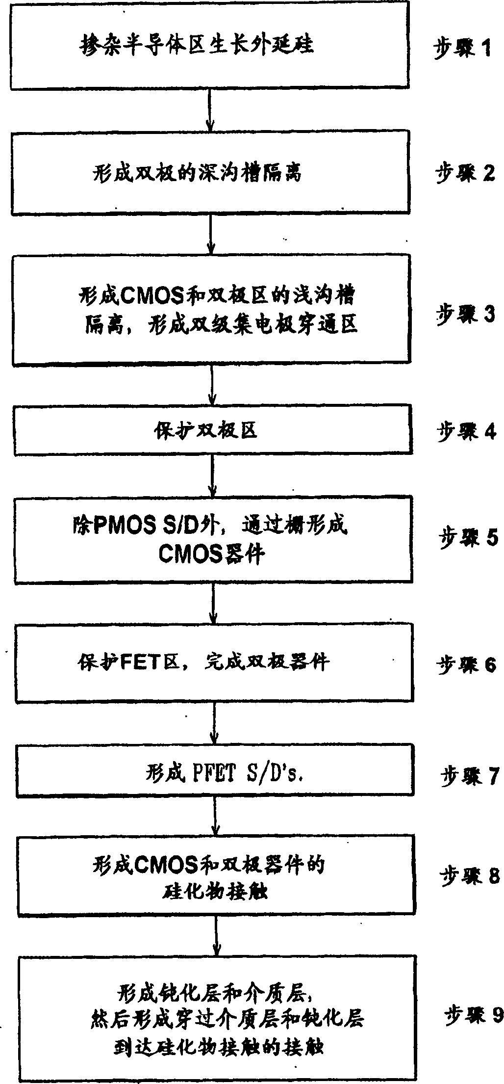
[0025] First, see figure 1 , which is a flow chart showing the basic processing steps of the integration scheme of the present invention. The steps shown in the flowcharts are described in greater detail below in conjunction with FIGS. 2A-2M and the discussion below.

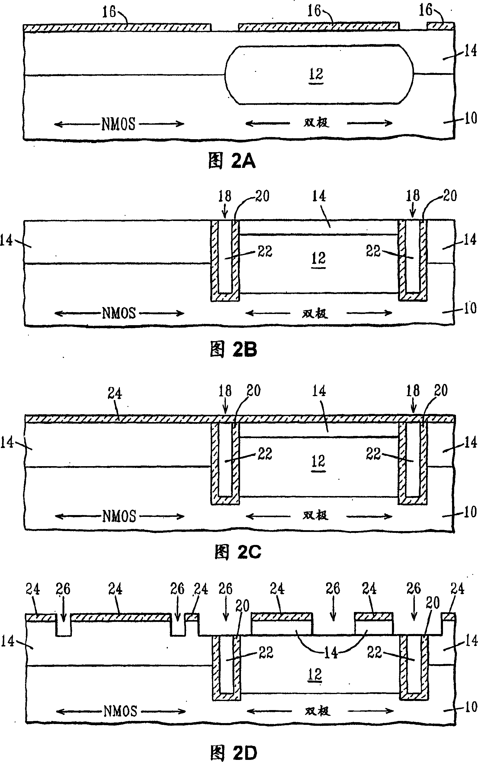
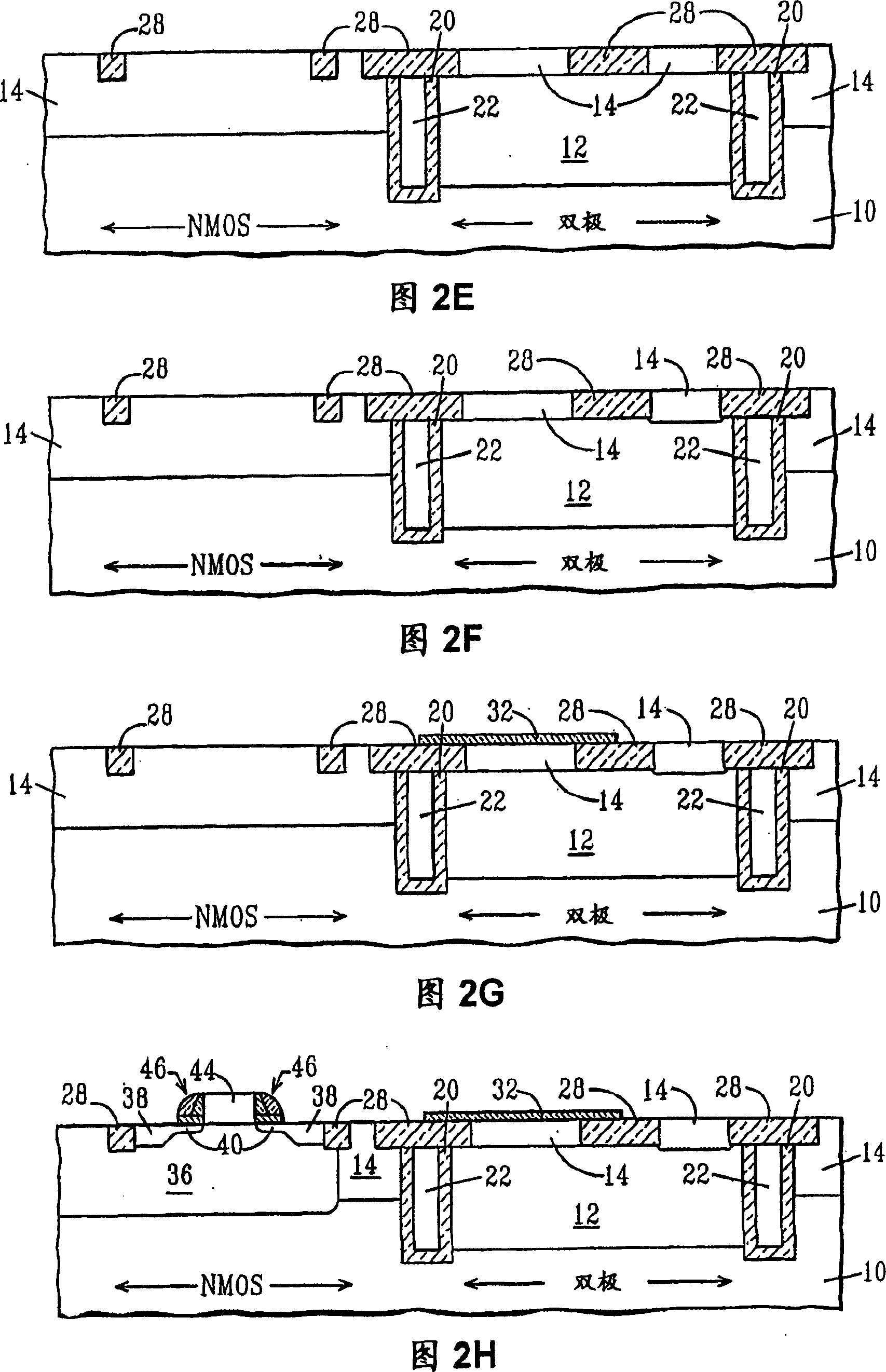
[0026] As shown in Figures 2A-2M, these figures are cross-sectional views of various processing steps employed in the present invention in the fabrication of BiCMOS structures including bipolar and NMOS devices. Although NMOS devices are shown and described, the present invention can be used to fabricate PMOS devices. In an embodiment where a PMOS device...


PUM

PropertyMeasurementUnit
Thicknessaaaaaaaaaa
Thicknessaaaaaaaaaa

Abstract

A method of forming a semiconductor integrated circuit such as a BiCMOS integrated circuit comprises the steps of: (a) forming a first portion of a bipolar device in a first region of a substrate; (b) forming a first protective layer over the first region to protect the first portion of the bipolar devices; (c) forming field effect transistor devices in second regions of the substrate; (d) forming a second protective layer over the second regions of the substrate to protect the field effect transistor devices; (e) removing the first protective layer; (f) forming a second portion of the bipolar devices in the first region of the substrate; and (g) removing the second protective layer.

Description

technical field [0001] The present invention relates to a method of fabricating integrated circuits, and in particular to a method of forming field effect transistors (FETs) and bipolar devices on the same substrate. More specifically, the present invention provides an integrated solution capable of fabricating base-after gate BiCMOS (ie, bipolar devices and complementary metal-oxide-semiconductor (CMOS) devices) integrated circuits, which solves general and existing problems. There are issues related to integration scenarios. Background technique [0002] In the field of semiconductor device fabrication, it is well known that BiCMOS integrated circuits can be fabricated using a so-called base-during gate process. For example, in D.L. Harame et al., "Si / SiGe Epitaxial-Base Transistors-Part I: Materials Physics and Circuits" (IEEE. Trans. Elect. Devices, pp. 469-482, March 1995 ), D.L. Harame et al., "Si / SiGe Epitaxial-Base Transistors-Part II: Process Integration and Analo...

Claims


Application Information

Patent Timeline
IPC IPC(8): H01L21/762H01L21/328H01L21/763H01L21/8222H01L21/8248H01L21/8249H01L27/06
CPCH01L21/76224H01L21/763H01L21/8249H01L27/0623
Inventor D·D·库尔鲍J·S·顿恩P·J·盖斯P·B·格雷D·L·哈拉梅K·T·舍内伯格S·A·斯特安格S·苏班纳
Owner IBM CORP
Why Eureka
Try Eureka