Temporary adhesive for wafer processing, wafer laminate, and method for manufacturing thin wafer
A temporary bonding and wafer processing technology, which is applied in semiconductor/solid-state device manufacturing, adhesives, adhesive additives, etc., can solve the problems of cleaning and removal, difficult to apply manufacturing technology, and long time, etc., to achieve cleaning and removal Excellent performance, excellent durability, high heat resistance effect
- Summary
- Abstract
- Description
- Claims
- Application Information
AI Technical Summary
Problems solved by technology
Method used
Image
Examples
Embodiment
[0127] Hereinafter, preparation examples, comparative preparation examples, examples, and comparative examples are shown to describe the present invention more specifically, but the present invention is not limited to these examples. In addition, the viscosity is the measured value at 25 degreeC using a rotational viscometer.
[0128] [1] Preparation of thermosetting silicone resin solution
preparation example 1
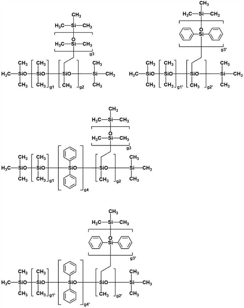
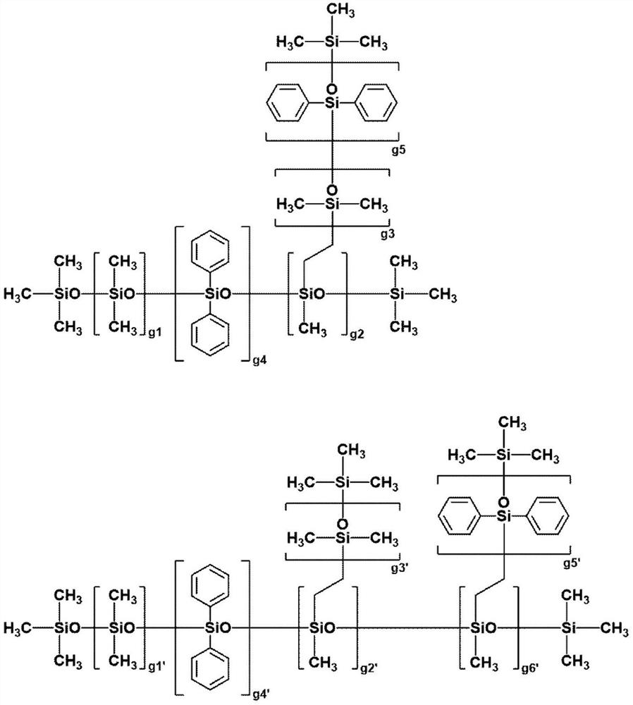
[0130] To a solution composed of 100 parts by mass of dimethylpolysiloxane having 2.5 mol % of vinyl groups in molecular side chains, 30,000 Mn, and 200 parts by mass of toluene, add: 50 parts by mass of 50 mol % of SiO 4 / 2 unit (Q unit), 48 mol% of (CH 3 ) 3 SiO 1 / 2 units (M units) and 2 mol% of (CH 2 =CH) 3 SiO 1 / 2 Units (Vi units), a solution composed of vinylmethylpolysiloxane with Mn of 7000 and 100 parts by mass of toluene, 230 parts by mass of organic hydrogen represented by the following formula (M-1) with Mn of 2800 Polysiloxane, a linear dimethylpolysiloxane having a viscosity (25° C.) of 30,000 mPa·s from 50 parts by mass of a 30 mass % toluene solution and having both ends of the molecular chain blocked by trimethylsiloxy groups A solution consisting of 120 parts by mass of toluene and 0.6 part by mass of 1-ethynylcyclohexanol were mixed. Furthermore, 0.4 parts by mass of a hydrosilylation reaction catalyst CAT-PL-5 (manufactured by Shin-Etsu Chemical Co., L...
preparation example 2
[0134] 70 parts by mass of dimethylpolysiloxane having 2.5 mol % of vinyl groups in molecular side chains and Mn of 30,000, and 30 parts by mass of dimethyl polysiloxane having 0.15 mol % of vinyl groups in both terminal chains and Mn of 60,000 To a solution consisting of dimethylpolysiloxane and 200 parts by mass of toluene, add: 50 parts by mass of SiO containing 50 mol % 4 / 2 unit (Q unit), 48 mol% of (CH 3 ) 3 SiO 1 / 2 units (M units) and 2 mol% of (CH 2 =CH) 3 SiO 1 / 2 Unit (Vi unit), a solution composed of vinylmethylpolysiloxane having Mn of 7000 and 100 parts by mass of toluene, 180 parts by mass of organohydrogenpolysilicon having Mn of 2800 represented by formula (M-1) Oxane, 30 parts by mass of a 30 mass % toluene solution having a viscosity (25° C.) of 1000 mPa·s, linear dimethylpolysiloxane having both ends of the molecular chain blocked by trimethylsiloxy groups, and 0.6 parts by mass of 1-ethynylcyclohexanol, and then mixed. Further, 0.4 parts by mass of a h...
PUM
| Property | Measurement | Unit |
|---|---|---|
| viscosity | aaaaa | aaaaa |
| viscosity | aaaaa | aaaaa |
| viscosity | aaaaa | aaaaa |
Abstract
Description
Claims
Application Information
 - R&D
- Intellectual Property
- Life Sciences
- Materials
- Tech Scout
- Unparalleled Data Quality
- Higher Quality Content
- 60% Fewer Hallucinations
Browse by: Latest US Patents, China's latest patents, Technical Efficacy Thesaurus, Application Domain, Technology Topic, Popular Technical Reports.
© 2025 PatSnap. All rights reserved.Legal|Privacy policy|Modern Slavery Act Transparency Statement|Sitemap|About US| Contact US: help@patsnap.com


