


Quick Research
Generate reliable direction feasibility study reports for your R&D in just a few steps.

Technical Q&A
Discover and master advanced knowledge NOW. Basics, ideas, possibilities, all at once.

Find Solutions
As an expert in R&D theories, this can generate solutions to your technical problems instantly.

Evaluate Feasibility
Analyze your overall solution with one click, know your potential R&D risks in advance.

Monitor Landscape
Get weekly tech updates, stay abreast of the latest tech innovations and key insights.
Heat dissipation type packaging structure and forming method thereof
A packaging structure and heat dissipation technology, applied in the direction of semiconductor/solid-state device parts, semiconductor devices, electrical components, etc., can solve the problems of chip damage, chip micro-cracks, etc., to improve the stability and prevent the overflow of glue.
- Summary
- Abstract
- Description
- Claims
- Application Information
AI Technical Summary
Problems solved by technology
Method used
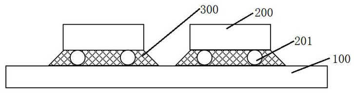
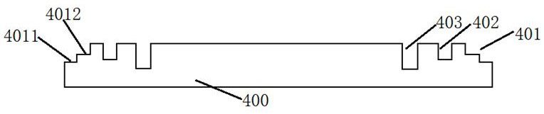
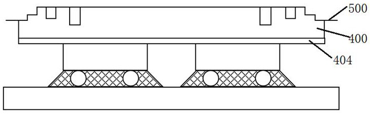
Image

Examples
Embodiment Construction
[0018] In order to better understand the technical solutions of the present invention, the embodiments of the present invention are described in detail below with reference to the accompanying drawings.
[0019] It should be understood that the described embodiments are only some, but not all, embodiments of the present invention. Based on the embodiments of the present invention, all other embodiments obtained by those of ordinary skill in the art without creative efforts shall fall within the protection scope of the present invention.
[0020] see Figure 1 to Figure 4 . It should be noted that the diagrams provided in this embodiment are only to illustrate the basic concept of the present invention in a schematic way, so the diagrams only show the components related to the present invention rather than the number, shape and the number of components in the actual implementation. For dimension drawing, the type, quantity and proportion of each component can be changed at wi...
PUM
 Abstract
Description
Claims
Application Information
 - R&D Engineer
- R&D Manager
- IP Professional
- Industry Leading Data Capabilities
- Powerful AI technology
- Patent DNA Extraction
Browse by: Latest US Patents, China's latest patents, Technical Efficacy Thesaurus, Application Domain, Technology Topic, Popular Technical Reports.
© 2024 PatSnap. All rights reserved.Legal|Privacy policy|Modern Slavery Act Transparency Statement|Sitemap|About US| Contact US: help@patsnap.com