Power supply boost drive circuit based on self-oscillation
A technology of self-excited oscillation and power boosting, which is applied in the direction of high-efficiency power electronic conversion, electrical components, and adjustment of electrical variables, etc., can solve the problems of large power supply and high cost, and achieve small circuit size, reduced peripheral components, and output The effect of voltage adjustment
- Summary
- Abstract
- Description
- Claims
- Application Information
AI Technical Summary
Problems solved by technology
Method used
Image
Examples
Embodiment 1
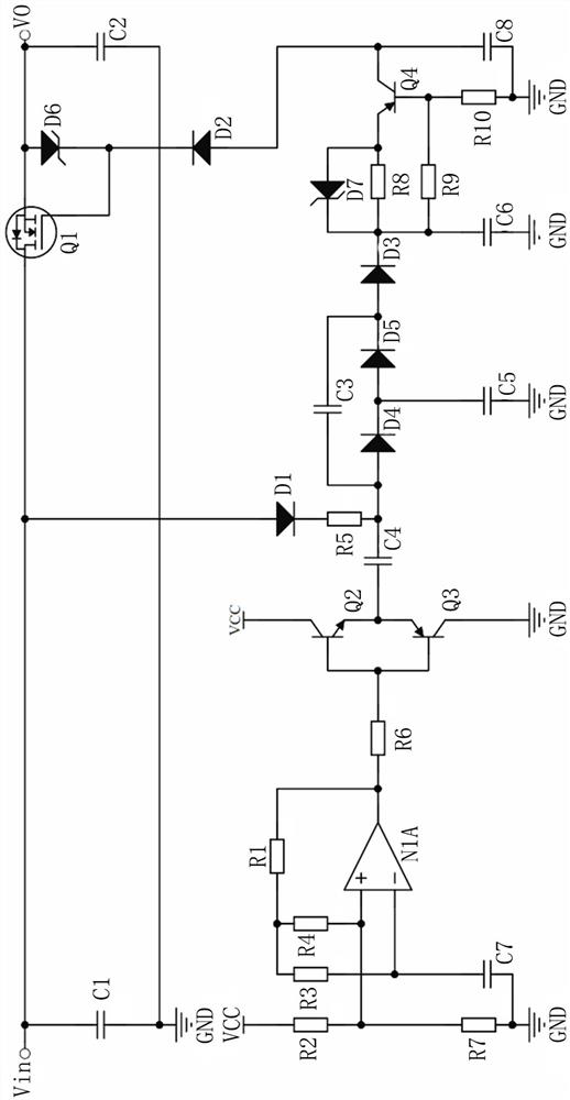
This embodiment provides a boost driving application, and its circuit schematic diagram is as follows figure 1 As shown, the circuit input voltage Vin is 28V, VCC is 10V, and the required output voltage VO is 27.75±0.25V. At this time, the circuit works as follows:
State 1: When Vin is powered and VCC is not powered, the oscillator does not work. Vin charges capacitor C6 and capacitor C8 through diode D1, resistor R5, diode D3, resistor R8 and transistor Q4. When the voltage of capacitor C6 reaches 26.6V, the capacitor The voltage on C8 reaches 26.3V, the charging reaches balance, the voltage on the capacitor C8 drives the MOS transistor Q1, and the output voltage VO is 22.6V.
[0025] State 2: When Vin and VCC supply power at the same time, the oscillator starts to work. If the oscillator output is high at the start of oscillation, the circuit working state is consistent with state 1, and the output voltage VO is 22.6V.
[0026] State 3: If the oscillator output is low at th...
Embodiment 2
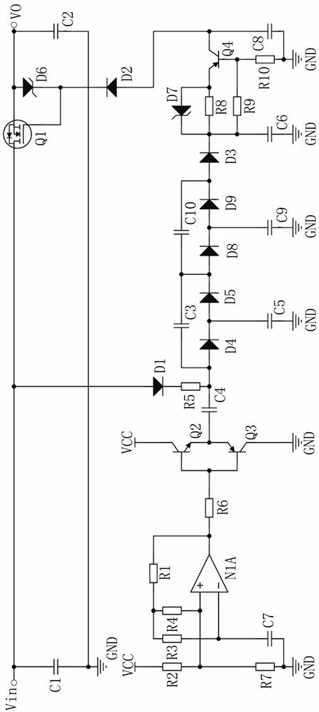
This embodiment provides a secondary boost driving application, and its circuit schematic diagram is as follows figure 2 As shown, at this time, the circuit input voltage Vin is 28V, VCC is 5V, and the required output voltage VO is 27.75±0.25V. At this time, the circuit works as follows:
State 1: When Vin is powered and VCC is not powered, the oscillator does not work. Vin charges capacitor C5, capacitor C6 and capacitor C8 through diode D1, resistor R5, diode D4, diode D5, diode D3, resistor R8 and transistor Q4. When the voltage of capacitor C5 reaches 26.6V, the voltage of capacitor C6 reaches 25.2V, the voltage on capacitor C8 reaches 24.9V, the charging is balanced, the voltage on capacitor C8 drives MOS transistor Q1, and the output voltage VO is 21.2V.
[0031] State 2: When Vin and VCC supply power at the same time, the oscillator starts to work. If the oscillator output is high at the start of oscillation, the circuit working state is the same as that of state 1, and...
Embodiment 3
This embodiment provides a three-time boost driving application, and its circuit schematic diagram is as follows image 3 As shown, the input voltage Vin of the circuit is 28V, VCC is 5V, and the required output voltage VO is 27.75±0.25V. The working principle of the circuit is as follows:
State 1: When Vin is powered and VCC is not powered, the oscillator does not work, Vin passes diode D1, resistor R5, diode D4, diode D5, diode D8, diode D9, diode D3, resistor R8 and transistor Q4 to capacitor C5, capacitor C9, capacitor C6 and capacitor C8 are charged. When the voltage of capacitor C5 reaches 26.6V, the voltage of capacitor C9 reaches 25.2V, the voltage of capacitor C6 reaches 23.8V, and the voltage of capacitor C8 reaches 23.5V, the charging is balanced, and the voltage on capacitor C8 drives the MOS Tube Q1, the output voltage VO is 19.8V.
[0039] State 2: When Vin and VCC supply power at the same time, the oscillator starts to work. If the oscillator output is high at ...
PUM
 Abstract
Description
Claims
Application Information
 - R&D Engineer
- R&D Manager
- IP Professional
- Industry Leading Data Capabilities
- Powerful AI technology
- Patent DNA Extraction
Browse by: Latest US Patents, China's latest patents, Technical Efficacy Thesaurus, Application Domain, Technology Topic, Popular Technical Reports.
© 2024 PatSnap. All rights reserved.Legal|Privacy policy|Modern Slavery Act Transparency Statement|Sitemap|About US| Contact US: help@patsnap.com


