Through hole electrical performance optimization design method and device, PCB and equipment
A technology of electrical performance and optimized design, applied in the direction of electrical components, electrical connection printed components, printed circuits, etc., can solve the problems of low electrical performance of through holes, increase the difficulty of processing, increase the difficulty of design, and improve the electrical performance of through holes. Effect
- Summary
- Abstract
- Description
- Claims
- Application Information
AI Technical Summary
Problems solved by technology
Method used
Image

Examples
Embodiment 1
[0035] The invention provides a method for optimizing the electrical performance of a through hole, including:
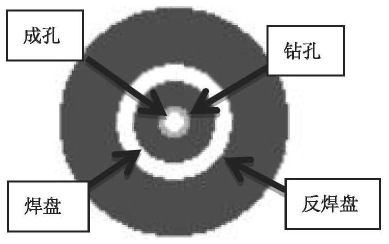
[0036] When the diameter of the pad and the diameter of the anti-pad remain unchanged, the copper plating ratio of the through hole is increased to improve the electrical performance of the through hole in the PCB board; where, the copper plating ratio=1-hole diameter / drilling diameter .
[0037] Among them, increasing the copper plating ratio of the through hole is specifically:
[0038] Keep the diameter of the drilled hole constant, and increase the copper plating ratio of the through hole by adjusting the size of the hole diameter; or, keep the hole diameter constant, and increase the copper plating ratio of the through hole by adjusting the size of the drilled hole diameter. After the increase, the copper plating ratio of the through hole is in the range of 0.3-0.4. Preferably, after the increase, the copper plating ratio of the through hole is 0.4.
[0039]...
Embodiment 2
[0062] The technical solution of the present invention also provides a through-hole electrical performance optimization design device, including:
[0063] Adjust the module to increase the copper plating ratio of the through hole under the condition that the diameter of the pad and the diameter of the anti pad are unchanged, so as to improve the electrical performance of the through hole in the PCB board; where, the copper plating ratio=1-hole diameter / Drill hole diameter.
[0064] Among them, increasing the copper plating ratio of the through hole is specifically:
[0065] Keep the diameter of the drilled hole constant, and increase the copper plating ratio of the through hole by adjusting the size of the hole diameter; or, keep the hole diameter constant, and increase the copper plating ratio of the through hole by adjusting the size of the drilled hole diameter. After the increase, the copper plating ratio of the through hole is in the range of 0.3-0.4. Preferably, after...
Embodiment 3
[0072] The technical solution of the present invention also provides a PCB board, which is formed on the basis of adopting the method for optimizing the electrical performance of through-holes in Embodiment 1.
[0073] The copper plating ratio of the through hole in the PCB board is in the range of 0.3-0.4. Preferably, the copper plating ratio of the through holes is 0.4.
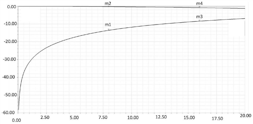
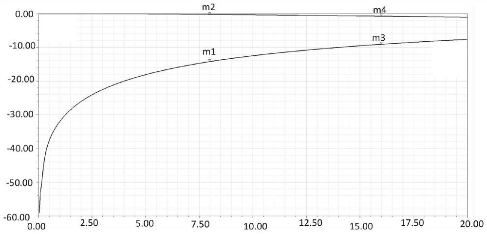
[0074] For example, in high-speed PCB board design, through holes of 8mil (hole diameter)-10mil (drilling aperture)-18mil (pad diameter)-28mil (anti-pad diameter) are usually used as the carrier of signal interconnection. For this kind of through hole, its copper plating ratio (Plating Ratio) is generally 1-8 / 10=0.2; Carry out replating to through hole (between hole and drilling), obtain new copper plating ratio, namely Ensure that the drill hole diameter (Drill Hole Diameter) remains unchanged at 10mil, and change the copper plating ratio to 0.3-0.4, that is, the corresponding finish hole diameter (Finish...
PUM
 Abstract
Description
Claims
Application Information
 - Generate Ideas
- Intellectual Property
- Life Sciences
- Materials
- Tech Scout
- Unparalleled Data Quality
- Higher Quality Content
- 60% Fewer Hallucinations
Browse by: Latest US Patents, China's latest patents, Technical Efficacy Thesaurus, Application Domain, Technology Topic, Popular Technical Reports.
© 2025 PatSnap. All rights reserved.Legal|Privacy policy|Modern Slavery Act Transparency Statement|Sitemap|About US| Contact US: help@patsnap.com