Integrated structure of graphene bypass diode and crystalline silicon solar cell and preparation method
A technology of crystalline silicon solar cells and diodes, applied in circuits, photovoltaic power generation, electrical components, etc., can solve the problems that the output power of photovoltaic modules is greatly affected and diodes cannot be integrated, so as to reduce leakage and heat generation, reduce output power and Safety impact, effect of reducing temperature rise
- Summary
- Abstract
- Description
- Claims
- Application Information
AI Technical Summary
Problems solved by technology
Method used
Image


Examples
preparation example Construction
[0061] The invention also discloses a method for preparing an integrated structure of a graphene bypass diode and a crystalline silicon solar cell, comprising:
[0062] Preparation of p on n-type silicon base region + type crystalline silicon emitter;
[0063] Prepare n on the backlight surface of the n-type silicon base region + silicon doped region;
[0064] in n + Isolation grooves are prepared on the silicon-doped region;
[0065] in n + A passivation layer is prepared on the silicon-doped region, and a backlight electrode window and a target window are opened on the passivation layer;
[0066] Transfer the graphene film layer on the target window, bake it with n + The silicon-doped region forms a Schottky junction;
[0067] Prepare a graphene surface electrode on the backlight surface of the graphene film layer;
[0068] Prepare the backlight electrode on the backlight electrode window;
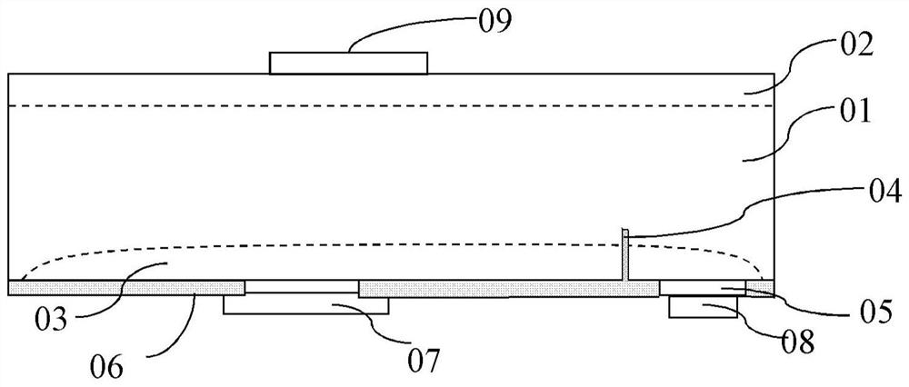
[0069] in p + The light-facing electrode is prepared on the emitter region...
Embodiment 1
[0091] In this embodiment, a method for preparing an integrated structure of a graphene bypass diode and a crystalline silicon solar cell is provided, including the following steps:
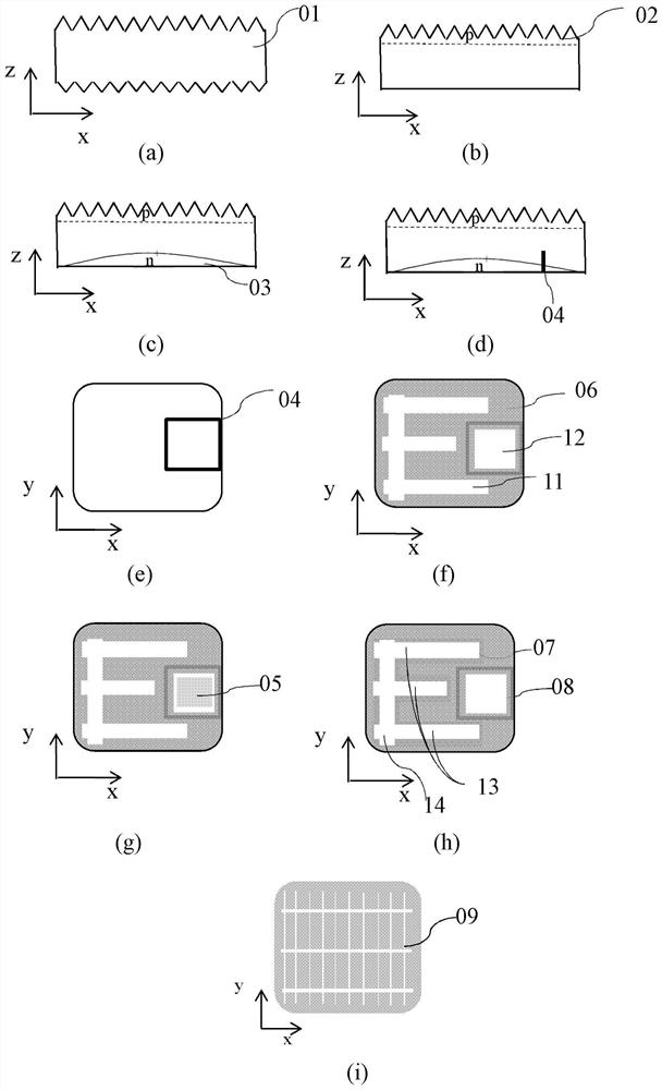
[0092] Such as figure 2 As shown in figure (a) in the middle, an n-type silicon wafer that has been cleaned and textured by a conventional process is provided as the n-type silicon base region 01 .
[0093] Such as figure 2 As shown in the figure (b), the front side of the n-type silicon wafer is subjected to a conventional boron diffusion process to form a p + For the crystalline silicon emission area 02, a conventional polishing process is performed on the backlight surface of the silicon wafer.
[0094] Such as figure 2 As shown in (c) figure, the phosphor paste is screen-printed on the back side of the silicon wafer to form n + Silicon heavily doped region 03.
[0095] Such as figure 2 As shown in (d) and (e), a laser is used to isolate an isolation region 10 with an area of 5 cm ...
Embodiment 2
[0101] The graphene diode wire connection and the integrated structure of the graphene bypass diode and the crystalline silicon solar cell described before and after form a topological structure such as Figure 3-4 shown.
[0102]In this embodiment, the way of connecting the crystalline silicon solar cells in series is as follows: the light-facing electrode 09 of the 1# crystalline silicon solar cell is connected to the back-light electrode 07 of the 2# crystalline silicon solar cell, and the 2# crystalline silicon solar cell The light-facing electrode 09 is connected to the back-light electrode 07 of the 3# crystalline silicon solar cell.
[0103] In this embodiment, the connection mode of the graphene bypass diode is: the backlight surface electrode 07 of the 1# crystalline silicon solar cell is connected to the graphene surface electrode 08 of the 2# crystalline silicon solar cell. That is, the n-type region of 2# graphene diode (ie n + The heavily doped silicon region (0...
PUM
| Property | Measurement | Unit |
|---|---|---|
| Depth | aaaaa | aaaaa |
Abstract
Description
Claims
Application Information
 - R&D
- Intellectual Property
- Life Sciences
- Materials
- Tech Scout
- Unparalleled Data Quality
- Higher Quality Content
- 60% Fewer Hallucinations
Browse by: Latest US Patents, China's latest patents, Technical Efficacy Thesaurus, Application Domain, Technology Topic, Popular Technical Reports.
© 2025 PatSnap. All rights reserved.Legal|Privacy policy|Modern Slavery Act Transparency Statement|Sitemap|About US| Contact US: help@patsnap.com