
Patsnap Eureka
For R&D, Patsnap Eureka makes reading and utilizing patents & technical documents easy.
Patsnap Eureka AIR
Designed for self-driven R&D workflows. Generate viable solutions, solve complex R&D challenges, empower your innovation with AI.

Patsnap Eureka Materials
Designed for material experts only. Revolutionize your material R&D, from search, analyze, to developing new materials.

TechResearch
Generate reliable direction feasibility study reports for your R&D in just a few steps.

TechSeek
Discover and master advanced knowledge NOW. Basics, ideas, possibilities, all at once.

TechMind
As an expert in R&D Theories, TechMind can generates customized viable solutions instantly.

TechRisk
Analyze your overall solution with one click, know your potential R&D risks in advance.

TechMonitor
Get weekly tech updates, stay abreast of the latest tech innovations and key insights.
Forming method of semiconductor structure
A technology of semiconductor and dielectric structure, applied in semiconductor devices, semiconductor/solid-state device manufacturing, electrical components, etc., can solve the problem of shrinking fin channel size, inability to meet device performance requirements, and reducing fin field effect transistor operating current, etc. question
- Summary
- Abstract
- Description
- Claims
- Application Information
AI Technical Summary
Problems solved by technology
Method used
Image

Examples
Embodiment Construction
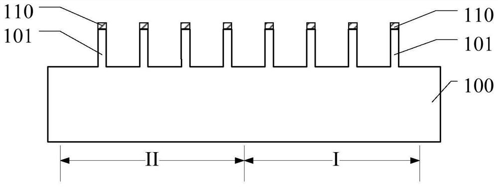
[0028] As mentioned in the background, in order to realize a semiconductor structure with strained fins to meet higher device density and meet device performance requirements, it is urgent to propose a semiconductor structure with strained fins Methods.
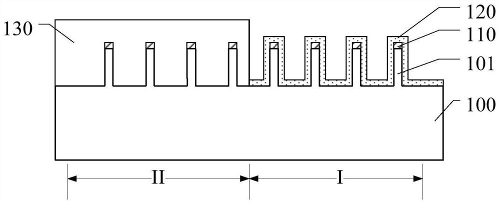
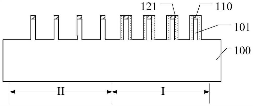
[0029] In order to solve the above problems, the technical solution of the present invention provides a method for forming a semiconductor structure, by forming a second strained fin on the sidewall surface of the initial first fin on the first region, and using the second strained fin as a mask, Etching the initial substrate and the initial first fins of the first region can form second invalid fins located between the substrate of the first region and the second strained fins, and, in each second invalid fin Between the adjacent second strained fins, an isolation opening extending into the second invalid fin is formed, which provides a method for forming a semiconductor structure with strained fins, and on this basis, the i...
PUM
 Abstract
Description
Claims
Application Information
 - R&D Engineer
- R&D Manager
- IP Professional
- Industry Leading Data Capabilities
- Powerful AI technology
- Patent DNA Extraction
Browse by: Latest US Patents, China's latest patents, Technical Efficacy Thesaurus, Application Domain, Technology Topic, Popular Technical Reports.
© 2024 PatSnap. All rights reserved.Legal|Privacy policy|Modern Slavery Act Transparency Statement|Sitemap|About US| Contact US: help@patsnap.com