FinFET integrated circuit basic unit
A basic unit and integrated circuit technology, which is applied in the field of microelectronics technology and integrated circuits, can solve the problems of Lch being unable to reduce the leakage-induced potential barrier, MOSFET channel length reduction, etc., to adjust the threshold voltage and reduce the conduction Resistance, the effect of boosting the accumulation effect
- Summary
- Abstract
- Description
- Claims
- Application Information
AI Technical Summary
Problems solved by technology
Method used
Image

Examples
Embodiment 1
[0055] Embodiment 1: Simulation and results of a highly doped nano-channel FinFET device.
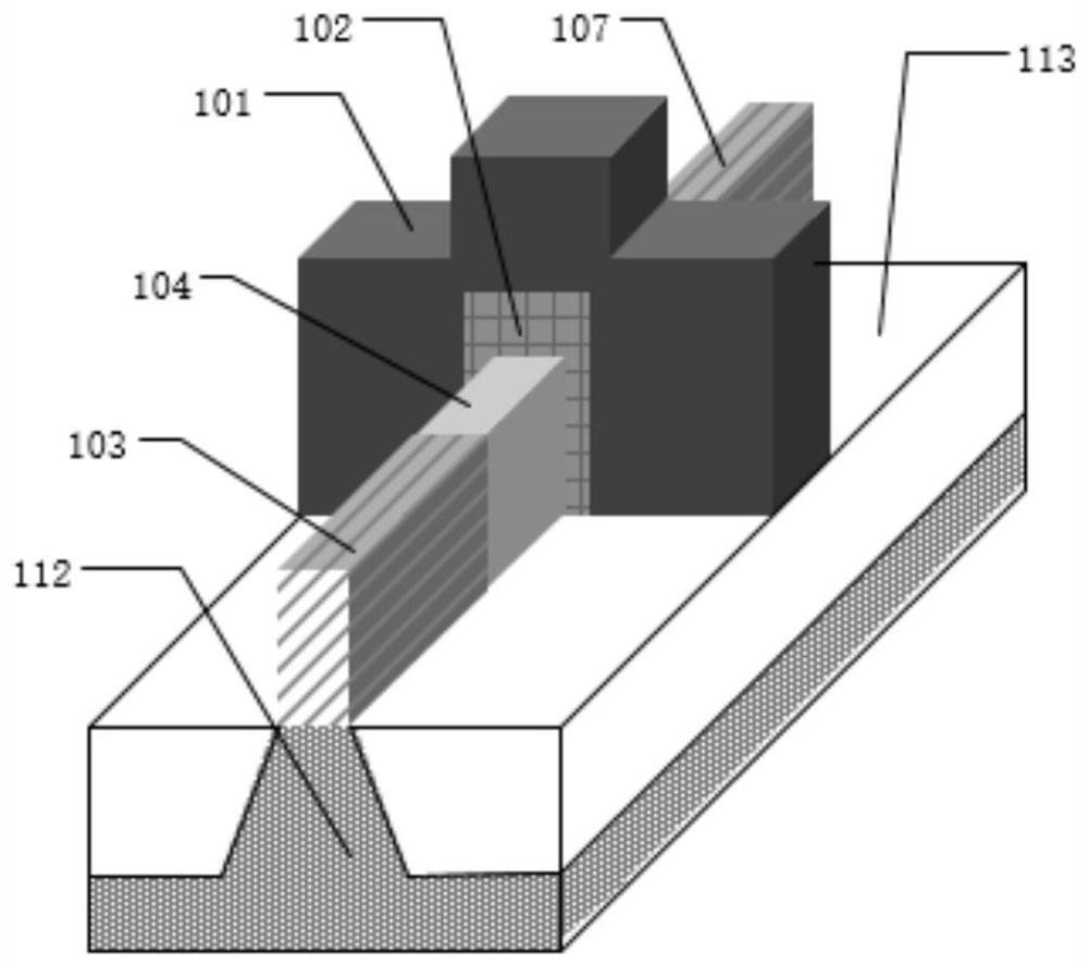
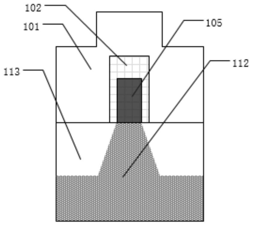
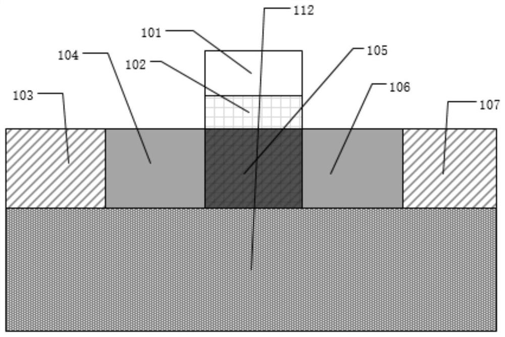
[0056] This embodiment emulates a kind of highly doped nano-channel FinFET device described in claim 1, and its output characteristic curve is as follows Figure 17 , the transfer characteristic curve as Figure 18 In this embodiment, the gate electrode (101) and the gate dielectric layer (102) only wrap the channel semiconductor region (105).
[0057] Taking the width in the horizontal direction and the thickness in the vertical direction, taking the NMOS with a thickness of 14nm in the 105 region as an example, the specific parameters of its structure are introduced. The thickness of the 103 region is 20nm, the width is 6nm, the material is silicon, and the doping concentration is 1x10 20 cm -3 , the impurity is phosphorus; the thickness of the 104 region is 3nm, the width is 6nm, the material is silicon, and the doping concentration is 5x10 15 cm -3 , the impurity is phosphorus;...
Embodiment 2
[0058] Embodiment 2: Simulation and results of a highly doped nano-channel FinFET device.
[0059] This embodiment emulates a highly doped nano-channel FinFET device described in claim 2, and its output characteristic curve is as follows Figure 23 , the transfer characteristic curve as Figure 24 , the difference of this embodiment lies in the way of wrapping the gate electrode and the gate dielectric layer. The gate electrode (101) and the gate dielectric layer (102) wrap the lightly doped drain region (106), the channel semiconductor region (105) and the lightly doped source region (104).
[0060] Taking the width in the horizontal direction and the thickness in the vertical direction, taking the NMOS with a thickness of 14nm in the 105 region as an example, the specific parameters of its structure are introduced. The thickness of the 103 region is 20nm, the width is 6nm, the material is silicon, and the doping concentration is 1x10 20 cm -3 , the impurity is phosphorus...
Embodiment 3
[0061] Embodiment 3: Simulation and results of a highly doped nano-channel FinFET device.
[0062] This embodiment emulates a highly doped nano-channel FinFET device described in claim 3, and its output characteristic curve is as follows Figure 25 , the transfer characteristic curve as Figure 26 , the maximum oscillation frequency curve is as Figure 27 , the maximum oscillation frequency is 1427GHz, the fixed voltage of lightly doped source region gate electrode (108) and lightly doped drain region gate electrode (110) is 0V; the difference of this embodiment is the material of gate electrode and gate dielectric layer with the wrapping method. The gate electrode (101) and the gate dielectric layer (102) wrap the channel semiconductor region (105), the lightly doped source region gate electrode (108) and the lightly doped source region gate dielectric layer (109) wrap the lightly doped source region region (104), the lightly doped drain region gate electrode (110) and the...
PUM
| Property | Measurement | Unit |
|---|---|---|
| relative permittivity | aaaaa | aaaaa |
Abstract
Description
Claims
Application Information
 - Generate Ideas
- Intellectual Property
- Life Sciences
- Materials
- Tech Scout
- Unparalleled Data Quality
- Higher Quality Content
- 60% Fewer Hallucinations
Browse by: Latest US Patents, China's latest patents, Technical Efficacy Thesaurus, Application Domain, Technology Topic, Popular Technical Reports.
© 2025 PatSnap. All rights reserved.Legal|Privacy policy|Modern Slavery Act Transparency Statement|Sitemap|About US| Contact US: help@patsnap.com