Circuit board and its manufacturing method and application
A production method and circuit board technology, which is applied in the fields of printed circuit manufacturing, printed circuit, and secondary treatment of printed circuit, etc., can solve the problems of increasing the haze of the circuit board, affecting the permeability and aesthetics of the circuit board, and improving the service life , to ensure the effect of stability and reliability
- Summary
- Abstract
- Description
- Claims
- Application Information
AI Technical Summary
Problems solved by technology
Method used
Image

Examples
Embodiment 1
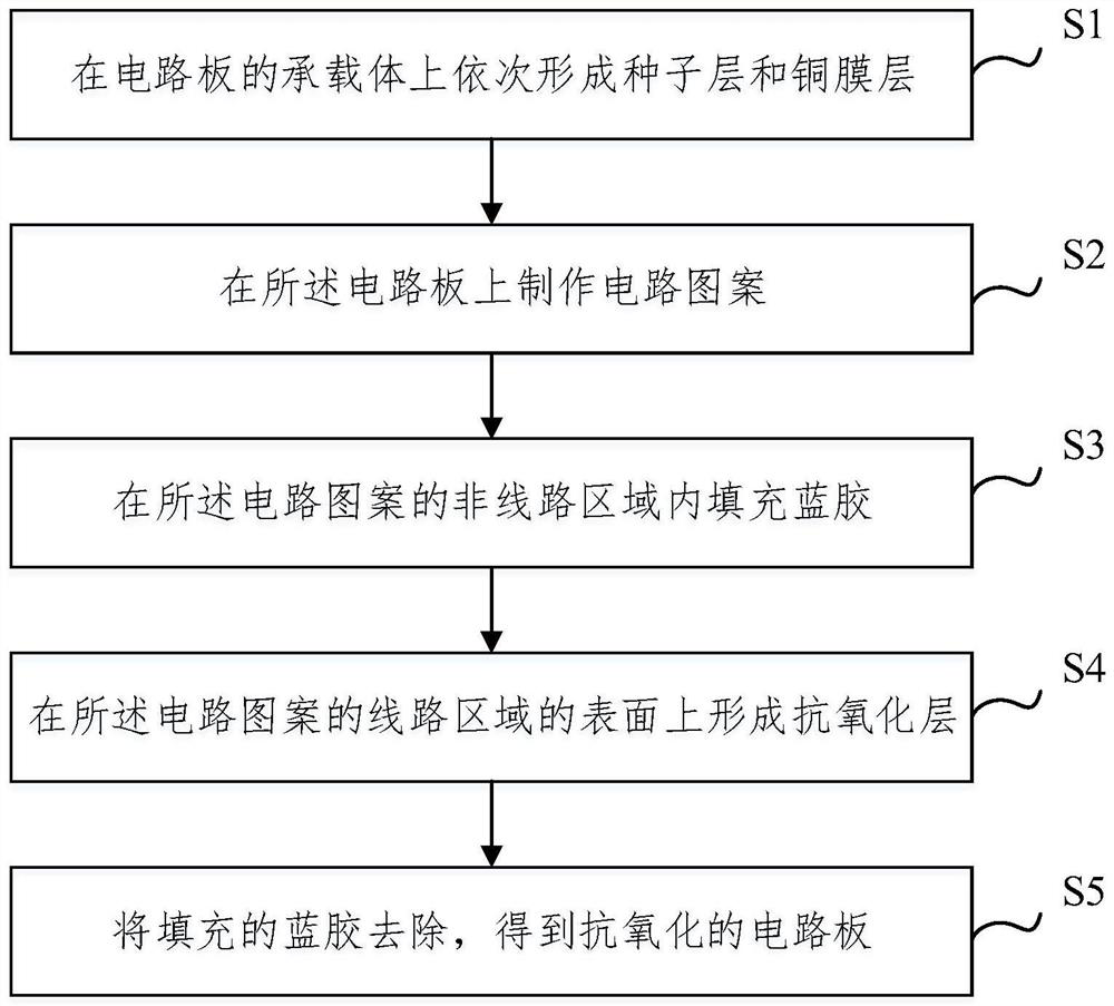
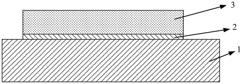
[0122] S0, using a glass plate as a circuit carrier, spraying the glass plate with a weak alkali cleaning solution (pH 7.1), cleaning with a rolling brush, rinsing with high-purity water, air-drying, and drying for subsequent use.
[0123] S1, a copper film layer 1 is sputtered on one surface of the glass plate by a magnetron sputtering process, the thickness is 10nm, and the process conditions are: the power density of the sputtering power supply is 2kw / cm 2 , the argon pressure is 0.6Pa, and the circuit board carrier temperature is 150°C;
[0124] On the surface of the copper film layer 1, the copper film layer 2 is electroplated by an acidic electroplating process, the thickness is 5 μm, and the process conditions are: pH value is 3, CuSO 4 Concentration is 20g / L, H 2 SO 4 The concentration is 160g / L, the chloride ion concentration is 100ppm, and the temperature is 30°C.
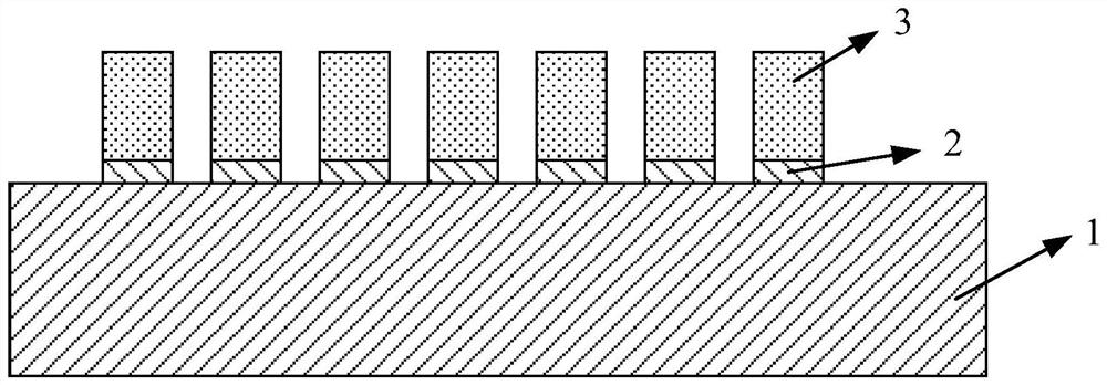
[0125] S2, Coating photoresist on the copper film layer 2 with a thickness of 10μm, designing a fil...
Embodiment 2
[0132] S0, the ceramic board is used as the circuit carrier, and the ceramic board is sprayed and cleaned with a weak acid cleaning solution (pH 6.2), washed with a rolling brush, rinsed with high-purity water, air-dried and dried, and used for standby.
[0133] S1, a copper-nickel alloy film layer is sputtered on one surface of the ceramic plate by magnetron sputtering process, the thickness is 20nm, and the process conditions are: sputtering power density 3kw / cm 2 , the pressure of argon gas is 0.7Pa, and the temperature of the circuit board carrier is 150°C;
[0134] On the surface of the copper-nickel alloy film layer, the copper film layer is electroplated by an acidic electroplating process, the thickness is 10 μm, and the process conditions are: pH value is 4, CuSO 4 Concentration is 30g / L, H 2 SO 4 The concentration is 140g / L, the chloride ion concentration is 80ppm, and the temperature is 30°C;
[0135] S2, Coating photoresist on the copper film layer with a thickn...
Embodiment 3
[0141] Basically the same as Example 1, the differences include:
[0142] The carrier in S0 is PET;
[0143] A circuit pattern is obtained after the etching process in S2 is completed.
[0144] After the blue glue is filled in the non-circuit area in S3, the photoresist on the circuit area is removed, and the photoresist is removed by mechanical tearing, and the circuit board is baked at a temperature of 150°C 5 minutes.
[0145] Using SMT technology on the circuit board obtained above, the LED lamp beads are attached to make an LED display screen. The transparency of the circuit board can reach more than 90%, the pull-out resistance of the film layer is 1N, the number of LED lamp beads per square meter is more than 10,000, the brightness is more than 7000 lumens, and the resolution of the overall display can be increased to P10 level; anti-oxidation life can reach more than 3 years; good product rate can reach more than 98%.
PUM
| Property | Measurement | Unit |
|---|---|---|
| thickness | aaaaa | aaaaa |
| thickness | aaaaa | aaaaa |
| thickness | aaaaa | aaaaa |
Abstract
Description
Claims
Application Information
 - R&D
- Intellectual Property
- Life Sciences
- Materials
- Tech Scout
- Unparalleled Data Quality
- Higher Quality Content
- 60% Fewer Hallucinations
Browse by: Latest US Patents, China's latest patents, Technical Efficacy Thesaurus, Application Domain, Technology Topic, Popular Technical Reports.
© 2025 PatSnap. All rights reserved.Legal|Privacy policy|Modern Slavery Act Transparency Statement|Sitemap|About US| Contact US: help@patsnap.com