Schottky gate field effect transistor based on two-dimensional size cutting and preparation method thereof
A field-effect transistor and Schottky gate technology, applied in the field of microelectronics, can solve problems such as lattice mismatch and increase process flow, achieve high reliability, simple process, and avoid random fluctuations
- Summary
- Abstract
- Description
- Claims
- Application Information
AI Technical Summary
Problems solved by technology
Method used
Image
Examples
Embodiment 1
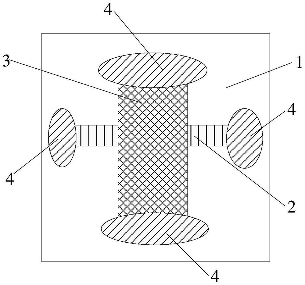
[0020] First, the structure of the Schottky gate field effect transistor in the present invention is introduced. refer to Figure 1A , 1B , which includes a substrate. In order to facilitate the distinction from other subsequent substrates, this substrate is referred to as the first substrate 1 herein. The first substrate 1 can be, for example, a sapphire substrate. Of course, for those skilled in the art Other types of substrates can also be used, and the present invention does not limit the types of substrates.
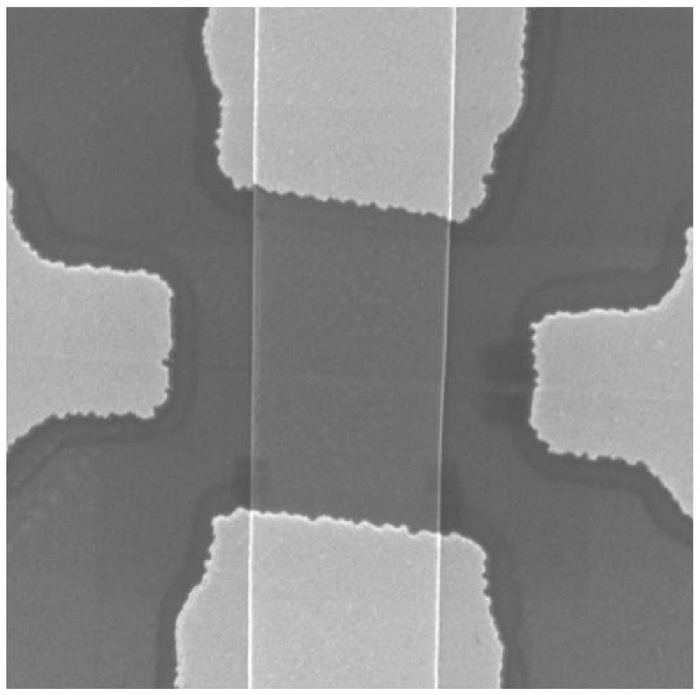
[0021] A two-dimensional material nanoribbon 2 is formed on a substrate 1 , and a bulk film 3 is located above the nanoribbon 2 and intersects with the nanoribbon 2 , for example, may be a cross. In FIG. 1 , the nanobelt 2 is in direct contact with the substrate 1 , and the bulk film 3 covers part of the nanobelt 2 and is perpendicular to the nanobelt 2 . The nanobelt 2 and the bulk film 3 are connected by intermolecular forces.
[0022] Metal electrodes 4 are fo...
Embodiment 2
[0027] This embodiment mainly introduces a manufacturing method of a Schottky gate field effect transistor, wherein the Schottky gate field effect transistor has the structure in Embodiment 1. The following will combine Figure 2A to Figure 5 The method in this embodiment is described in detail, which generally includes the following steps S1-S6.
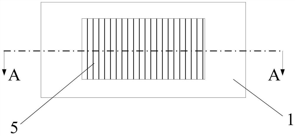
[0028] S1: forming a two-dimensional material thin film 5 on the first substrate 1 .
[0029] refer to Figure 2A and Figure 2B ,in Figure 2B for Figure 2A Sectional view along A-A direction. The first substrate 1 can be a sapphire substrate, and the two-dimensional material thin film 5 can be selected as a molybdenum disulfide thin film. For example, the sapphire with single-side polishing on the upper surface is selected as the sapphire substrate, and the mechanically peeled-off sapphire substrate is prepared on the sapphire substrate. A molybdenum disulfide thin film with a thickness of 1-20nm is used to obtain the first...
Embodiment 3
[0049] This embodiment focuses on the differences from other embodiments, and the similarities will not be repeated. refer to Figure 6 , different from the structure in Embodiment 1, in this embodiment a bulk film 3 is formed on the first substrate 1, and the two-dimensional material nanoribbon 2 is located above the bulk film 3 and intersects with the bulk film 3, for example, It's a cross. In FIG. 1 , the bulk film 3 is in direct contact with the substrate 1 , and the nanobelt 2 covers part of the bulk film 3 and is perpendicular to the bulk film 3 . The nanobelt 2 and the bulk film 3 are connected by intermolecular forces.
[0050] Same as Example 1, metal electrodes 4 are formed at both ends of the nanobelt 2 and the bulk film 3, and the same two-dimensional material can be used for the nanobelt 2 and the bulk film 3, for example, molybdenum disulfide can be used for both.
PUM
| Property | Measurement | Unit |
|---|---|---|
| thickness | aaaaa | aaaaa |
| width | aaaaa | aaaaa |
| diameter | aaaaa | aaaaa |
Abstract
Description
Claims
Application Information
 - R&D
- Intellectual Property
- Life Sciences
- Materials
- Tech Scout
- Unparalleled Data Quality
- Higher Quality Content
- 60% Fewer Hallucinations
Browse by: Latest US Patents, China's latest patents, Technical Efficacy Thesaurus, Application Domain, Technology Topic, Popular Technical Reports.
© 2025 PatSnap. All rights reserved.Legal|Privacy policy|Modern Slavery Act Transparency Statement|Sitemap|About US| Contact US: help@patsnap.com


