Silicon-based LED epitaxial structure and preparation method and application thereof

An epitaxial structure, silicon-based technology, applied in electrical components, circuits, semiconductor devices, etc., can solve the problems of increased time and cost, long emission wavelength, low temperature, etc., to achieve simple and fast operation, improve wavelength yield, save The effect of production cost

Pending Publication Date: 2021-11-30
广州市众拓光电科技有限公司
View PDF0 Cites 0 Cited by
  • Summary
  • Abstract
  • Description
  • Claims
  • Application Information

AI Technical Summary

Problems solved by technology

However, when the silicon base is used as the substrate, the stress caused by the lattice mismatch between the silicon substrate and GaN and the thermal deformation will cause the LED epitaxial wafer to warp, and the warping will make the subsequent growth of the light-emitting layer , the edge of the epitaxial wafer is closer to or close to the surface of the graphite disk than the center, so that the temperature of the central part is lower than that of the edge part, and finally the luminous wavelength of the central part of the epitaxial wafer after growing the light emitting layer is longer than that of the edge part
Especially when growing large-size LED epitaxial wafers, due to the large area, the wavelength difference between the central part and the edge part of the epitaxial wafer will be aggravated, and the wavelength uniformity of the epitaxial wafer will be reduced, which will affect the subsequent chip preparation process and sorting work. It will cause a substantial increase in time and cost, and will also lead to a significant decrease in the wavelength yield of LED epitaxial wafers

Method used


Image

  • Silicon-based LED epitaxial structure and preparation method and application thereof
  • Silicon-based LED epitaxial structure and preparation method and application thereof

Examples


Embodiment 1

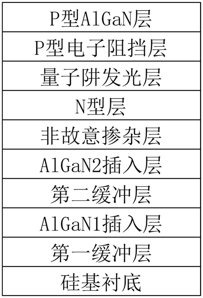
[0041] A silicon-based LED epitaxial structure, the silicon-based epitaxial structure includes a silicon-based substrate, a first buffer layer, an AlGaN1 insertion layer, a second buffer layer, an AlGaN2 insertion layer, an unintentionally doped layer, and an N-type layer from bottom to top , a quantum well light-emitting layer, a P-type electron blocking layer and a P-type AlGaN layer.

[0042] The preparation method of the silicon-based epitaxial structure comprises the following steps:

[0043] Step S1: prepare a silicon-based substrate, put the silicon-based substrate in 1000°C H 2 Baking under atmosphere for 1min;

[0044] Step S2: growing a first buffer layer on a silicon-based substrate; the growth temperature is 600° C., and the growth thickness is 20 nm;

[0045] Step S3: growing an AlGaN1 insertion layer on the first buffer layer at a growth temperature of 900°C;

[0046] Step S4: growing a second buffer layer on the AlGaN1 insertion layer at a growth temperature ...

Embodiment 2

[0054] A silicon-based LED epitaxial structure, the silicon-based epitaxial structure includes a silicon-based substrate, a first buffer layer, an AlGaN1 insertion layer, a second buffer layer, an AlGaN2 insertion layer, an unintentionally doped layer, and an N-type layer from bottom to top , a quantum well light-emitting layer, a P-type electron blocking layer and a P-type AlGaN layer.

[0055] The preparation method of the silicon-based epitaxial structure comprises the following steps:

[0056] Step S1: prepare a silicon-based substrate, put the silicon-based substrate in 1100°C H 2 Baking under the atmosphere for 2min;

[0057] Step S2: growing a first buffer layer on a silicon-based substrate; the growth temperature is 900° C., and the growth thickness is 100 nm;

[0058] Step S3: growing an AlGaN1 insertion layer on the first buffer layer at a growth temperature of 1100°C;

[0059] Step S4: growing a second buffer layer on the AlGaN1 insertion layer at a growth temper...

Embodiment 3

[0067] A silicon-based LED epitaxial structure, the silicon-based epitaxial structure includes a silicon-based substrate, a first buffer layer, an AlGaN1 insertion layer, a second buffer layer, an AlGaN2 insertion layer, an unintentionally doped layer, and an N-type layer from bottom to top , a quantum well light-emitting layer, a P-type electron blocking layer and a P-type AlGaN layer. Wherein the Al component content in the AlGaN1 insertion layer is 30%, and the Al component content in the AlGaN2 insertion layer is 15%. The preparation method is the same as in Example 1.


PUM

PropertyMeasurementUnit
Growth thicknessaaaaaaaaaa
Total thicknessaaaaaaaaaa

Abstract

The invention relates to the technical field of light emitting diodes, in particular to a silicon-based LED epitaxial structure and a preparation method and application thereof. The silicon-based epitaxial structure comprises a silicon-based substrate, a first buffer layer, an AlGaN1 insertion layer, a second buffer layer, an AlGaN2 insertion layer, an unintentional doping layer, an N-type layer, a quantum well light-emitting layer, a P-type electron blocking layer and a P-type AlGaN layer from bottom to top. By arranging the AlGaN1 insertion layer and the AlGaN2 insertion layer, the phenomenon that the LED epitaxial wafer warps due to stress generated by lattice mismatch and thermal deformation difference between the silicon-based substrate and GaN is avoided, warping of the silicon-based epitaxial structure is controlled, and then the wavelength yield is increased.

Description

technical field [0001] The invention relates to the technical field of light emitting diodes, in particular to a silicon-based LED epitaxial structure and a preparation method and application thereof. Background technique [0002] A light emitting diode (Light Emitting Diode, LED) is a commonly used light emitting device, which releases energy and emits light through the recombination of electrons and holes, and is widely used in the field of lighting. Light-emitting diodes can efficiently convert electrical energy into light energy, and have a wide range of uses in modern society, such as lighting, flat panel displays, medical devices, etc. [0003] MOCVD (Metal-Organic Chemical Vapor Deposition, metal-organic chemical vapor deposition) is a new type of vapor phase epitaxy growth technology developed on the basis of vapor phase epitaxy (Vapor Phase Epitaxy, VPE) growth. At present, most LED epitaxial wafers are prepared on other substrates by MOCVD technology. However, wh...

Claims


Application Information

Patent Timeline
IPC IPC(8): H01L33/12H01L33/00
CPCH01L33/12H01L33/007
Inventor 李国强
Owner 广州市众拓光电科技有限公司
Why Eureka
Try Eureka