
Method for reducing radio frequency loss caused by gallium diffusion in silicon-based gallium nitride material

A radio frequency loss, gallium nitride technology, applied in chemical instruments and methods, polycrystalline material growth, from chemically reactive gases, etc., can solve problems such as insufficient cleanliness, reduce radio frequency loss, reduce parasitic conductance, and suppress radio frequency The effect of loss

Pending Publication Date: 2021-11-30
PEKING UNIV
View PDF3 Cites 0 Cited by
  • Summary
  • Abstract
  • Description
  • Claims
  • Application Information

AI Technical Summary

Problems solved by technology

But that alone is still not enough cleanliness

Method used


Image

  • Method for reducing radio frequency loss caused by gallium diffusion in silicon-based gallium nitride material
  • Method for reducing radio frequency loss caused by gallium diffusion in silicon-based gallium nitride material
  • Method for reducing radio frequency loss caused by gallium diffusion in silicon-based gallium nitride material

Examples


Embodiment Construction

[0019] Below in conjunction with accompanying drawing, the present invention will be further described through embodiment.

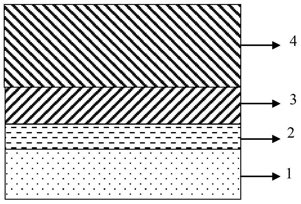
[0020] In order to solve the problem of radio frequency loss caused by the diffusion of residual gallium in silicon-based GaN radio frequency devices, the following comparative experiments were prepared figure 1 A sample of the structure shown:

[0021] In this embodiment, a high-resistance silicon substrate 1 is selected, the resistance value is 10 kiloohms cm (kΩ cm), and the thickness is 650 microns; the epitaxial growth equipment used is metal organic compound vapor phase epitaxy (MOCVD) equipment, wherein The reaction chamber type is a close-coupled shower (CCS) reaction chamber.

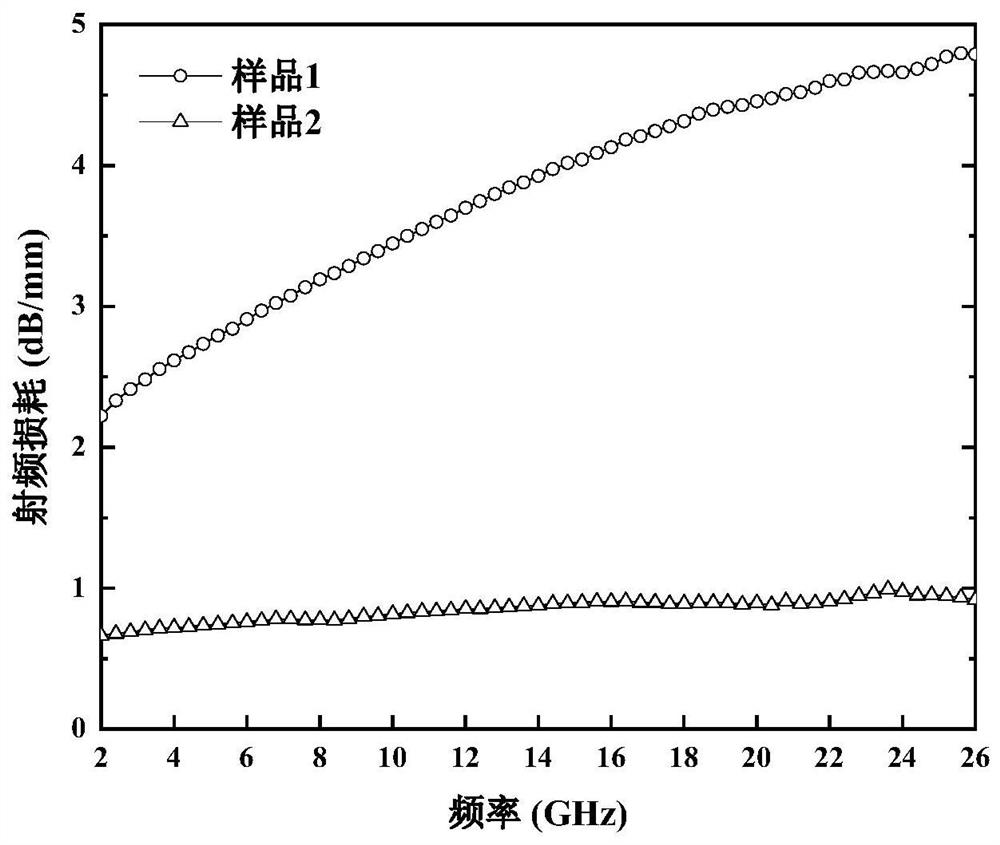
[0022] Preparation of sample 1: before the furnace of the required sample is formally grown, the reaction chamber is baked (bake), that is, the entire reaction chamber is baked at a temperature greater than 1000 ° C in a hydrogen atmosphere; then the high-resistance sili...


PUM

PropertyMeasurementUnit
thicknessaaaaaaaaaa
thicknessaaaaaaaaaa
thicknessaaaaaaaaaa

Abstract

The invention discloses a method for reducing radio frequency loss caused by gallium diffusion in a silicon-based gallium nitride material. Before epitaxial growth is carried out on a high-resistance silicon substrate, a furnace of AlN growth is carried out in advance, and a spray head, a graphite disc and the like in a reaction chamber are covered with AlN, so that residual Ga is effectively prevented from being diffused into the silicon substrate, parasitic conductance caused by holes introduced by Ga impurities at the interface of the silicon substrate and an epitaxial layer is further reduced, and the radio frequency loss of the silicon-based gallium nitride radio frequency device is reduced. According to the method, radio frequency loss caused by diffusion of residual Ga to the silicon substrate in the epitaxial process of the GaN material on the silicon substrate can be effectively inhibited, and the method plays an important role in improving the performance of a silicon-based gallium nitride radio frequency device.

Description

technical field [0001] The invention belongs to the technical field of semiconductors, and in particular relates to a method for solving the radio frequency loss problem faced by silicon-based gallium nitride radio frequency devices in application. Background technique [0002] Group III nitride semiconductors represented by gallium nitride (GaN) have excellent properties such as large band gap, high breakdown electric field, high saturation electron drift velocity, and strong polarization effect, especially based on silicon (Si) substrates. High electron mobility transistor (HEMT) with aluminum gallium nitride / gallium nitride (AlGaN / GaN) heterostructure on silicon carbide (SiC) substrate has high power density, small device size, high temperature resistance and high frequency Excellent characteristics such as low-level applications, so it has great potential in the field of radio frequency power devices. [0003] The current commercialized GaN-based RF power devices genera...

Claims


Application Information

Patent Timeline
Patent Type & Authority Applications(China)
IPC IPC(8): H01L21/02C30B25/18C30B29/40
CPCH01L21/02381H01L21/0254H01L21/02458H01L21/0262C30B25/183C30B29/403C30B29/406
Inventor 杨学林沈波马骋刘丹烁蔡子东陈正昊
Owner PEKING UNIV
Learn More