Silicon photon pin junction light attenuation structure

A silicon photonics and optical attenuation technology, applied in optics, nonlinear optics, instruments, etc., can solve the problems of slow response, high cost, polarization-related loss, etc., and achieve the effect of wide attenuation range and fast response

Pending Publication Date: 2021-11-19
CENT SOUTH UNIV
View PDF6 Cites 0 Cited by
  • Summary
  • Abstract
  • Description
  • Claims
  • Application Information

AI Technical Summary

Problems solved by technology

[0007] Patent ZL201910413070.2 (adjustable optical attenuator and control method), patent ZL201310216150.1 (planar waveguide type adjustable optical attenuator), utility model ZL201821388443.2 (a silicon-based silica thermo-optic adjustable optical attenuator ), patent ZL201610024461.1 (a PLC-type adjustable optical attenuator and its method for improving temperature correlation), utility model ZL201520835273.8 (a silicon-based silicon dioxide thermo-optic adjustable optical attenuator) and other patents are all It is based on the thermo-optic tunable principle of MZI to realize the attenuation of light. Although the structure is simple and low in cost, the response is slow; and due to different materials and different thermal expansion coefficients, stress will be generated, which will lead to polarization-dependent loss.
[0008] Patent 201510506308.8 (graphene phase-type optical modulator based on planar waveguide) proposes a graphene phase-type optical modulator based on planar waveguide. This structure can also be applied to light attenuation, but the graphene layer is difficult to manufacture in batches with high quality. and higher cost

Method used


Image

  • Silicon photon pin junction light attenuation structure
  • Silicon photon pin junction light attenuation structure
  • Silicon photon pin junction light attenuation structure

Examples


Embodiment Construction

[0031] It should be noted that, in the case of no conflict, the embodiments in the present application and the features in the embodiments can be combined with each other. The present application will be described in detail below with reference to the accompanying drawings and embodiments.

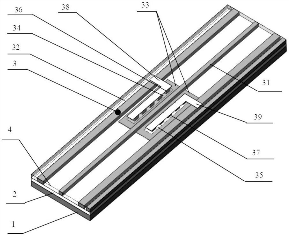
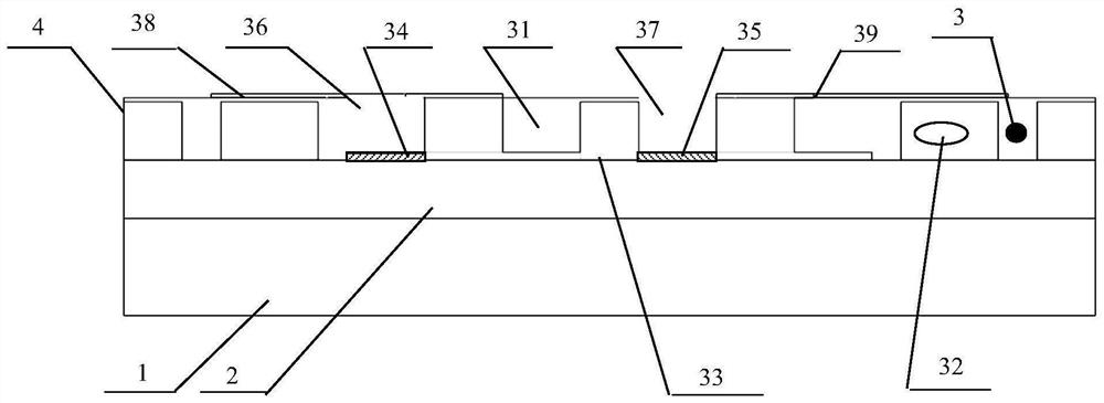
[0032] In this embodiment, a silicon photonic pin junction light attenuation structure is provided. The silicon photonic pin junction light attenuation structure is made on the basis of an SOI wafer. The SOI wafer includes: a base layer, a buried oxide layer and a device layer, wherein the device After the layer is etched, at least the first part remains, and the device layers on both sides of the first part are etched away, and the first part is the silicon light transmission waveguide; the two sides of the silicon light transmission waveguide respectively form a first step and a second step, wherein, The first step is ion implantation or diffusion step, and the second step is ion implant...


PUM


Abstract

The invention discloses a silicon photon pin junction light attenuation structure. The silicon photon pin junction light attenuation structure is made based on an SOI wafer. The SOI wafer comprises a substrate layer, a buried oxide layer and a device layer, at least a first part is left after the device layer is etched, and the first part is a silicon light transmission waveguide; a first step and a second step are respectively formed on two sides of the silicon optical transmission waveguide; a P region and / or an N region is formed on the first step, and an N region and / or a P region is formed on the second step; a metal interconnection column is formed on the P region, and a metal interconnection column is formed on the N region; a metal interconnection layer is formed on one of the P regions; and a metal interconnect layer is formed on one of the N regions. The problems existing in an adjustable light attenuation structure in the prior art are solved, and therefore the adjustable light attenuation structure which is wide in attenuation range and fast in response is provided.

Description

technical field [0001] This application relates to the field of optical chips, in particular, to a silicon photonic pin junction light attenuation structure. Background technique [0002] The variable optical attenuator (VOA, Variable Optical Attenuation) plays an important role in the optical fiber communication network. It forms a gain-balanced optical amplifier with an erbium-doped fiber amplifier (EDFA); it forms a gain controller with an amplified spontaneous emission (ASE) light source; Reconfiguring optical add-drop multiplexer (ROADM) to form a gain-balanced ROADM; figure 1 It is a schematic diagram according to the VOA channel equalization in the prior art; as figure 1 As shown, form a gain balancing MUX / DEMUX etc. with a multiplexer / demultiplexer (MUX / DEMUX). Therefore, VOA is one of the indispensable key components of optical fiber communication system. [0003] VOA has discrete and integrated types. The discrete type is composed of optical fibers, lenses, actu...

Claims


Application Information

Patent Timeline
Patent Type & Authority Applications(China)
IPC IPC(8): G02F1/025G02F1/015
CPCG02F1/025G02F1/0152
Inventor 郑煜唐昕段吉安
Owner CENT SOUTH UNIV
Why Eureka
Try Eureka