Substrate bearing combined multilayer film on surface, X-ray detector and preparation method of X-ray detector
A multi-layer film and detector technology, applied in semiconductor devices, final product manufacturing, sustainable manufacturing/processing, etc., can solve problems such as substrate temperature rise, substrate damage, and weak X-ray blocking and absorption capabilities, and achieve low leakage current Effects of density, strong X-ray absorption
- Summary
- Abstract
- Description
- Claims
- Application Information
AI Technical Summary
Problems solved by technology
Method used
Image
Examples
Embodiment 1
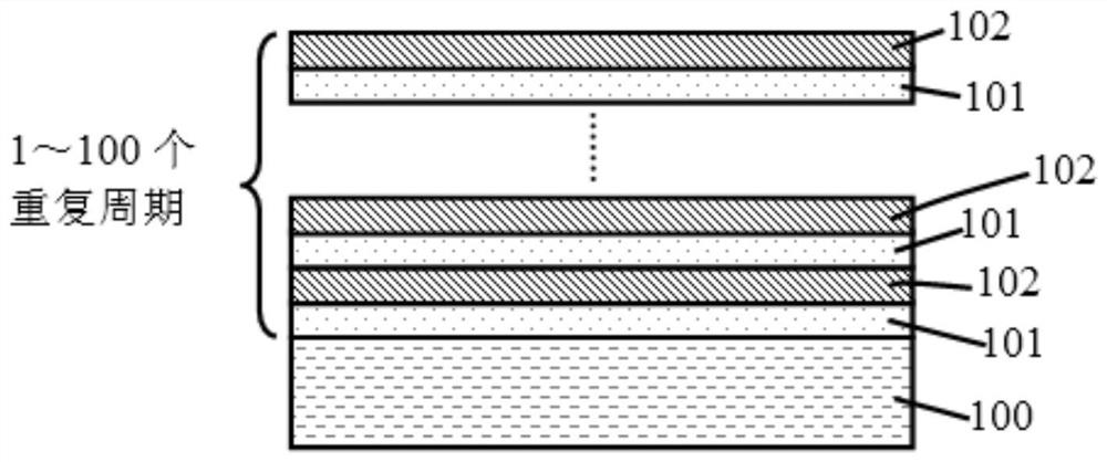
[0058] This embodiment provides a substrate with a combined multilayer film on its surface (refer to figure 2 shown), its preparation method refers to figure 1 shown.
[0059] Including from bottom to top: substrate 100, PbO layer 101 and Ga 2 o 3 Layer 102. The combined multilayer film is deposited on the surface of the substrate, the combined multilayer film refers to the PbO layer and the Ga 2 o 3 A multilayer film composed of repeating units stacked within a repetition frequency. The repetition frequency is 1-100.
[0060] In this embodiment, the thickness of each layer of PbO layer is set to be 2 microns, each layer of Ga 2 o 3 The thickness is 1 micron, that is to say PbO / Ga 2 o 3 The total thickness of the repeating unit is 3 microns, and the repeating frequency is 10, resulting in PbO-Ga 2 o 3 The combined multilayer film has a total thickness of 30 microns.
[0061] The absorption rate of X-ray photons with a tube voltage of 60kV is 63.8% by detecting th...
Embodiment 2
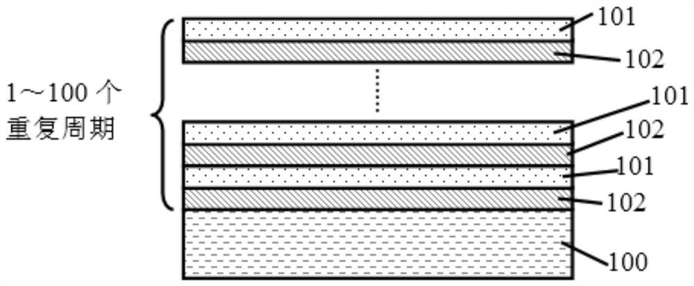
[0065] This embodiment provides a substrate with a combined multilayer film on its surface (refer to image 3 shown), its preparation method refers to figure 1 shown.
[0066] Including from bottom to top: substrate 100, Ga 2 o 3 layer 102 and PbO layer 101. The combined multilayer film is deposited on the surface of the substrate, the combined multilayer film refers to the PbO layer and the Ga 2 o 3 A multilayer film composed of repeating units stacked within a repetition frequency. The repetition frequency is 1-100.
Embodiment 3
[0068] This embodiment provides an X-ray detector, referring to Figure 4 shown, its preparation method refers to figure 1 shown.
[0069] The X-ray detector comprises from bottom to top: a substrate 100, a bottom electrode 103, a PbO layer 101, a Ga 2 o 3 layer 102 and top electrode 104.
[0070] Preparation methods include:
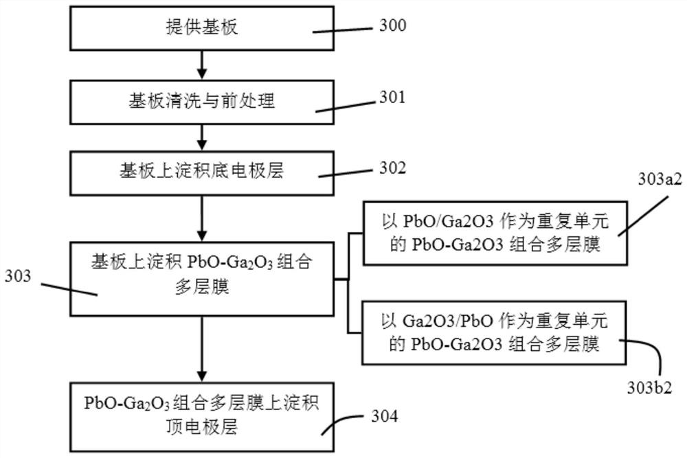
[0071] (1) Cleaning and pretreatment of the substrate, use electronic glass, soak it in dilute nitric acid for 2 minutes, rinse it with deionized water after taking it out, put it in an acetic acid solution for ultrasonic vibration cleaning for 10 minutes, and rinse it with absolute ethanol after taking it out, Soak it in acetone solution for 10 minutes, take it out and dry it with high-purity nitrogen. Put the cleaned substrate into the ultraviolet ozone cleaning machine for 1 minute, take it out and put it into the plasma cleaning machine, choose medium or high power to clean for 10 minutes, and put the substrate into the dust-free transfer box a...
PUM
| Property | Measurement | Unit |
|---|---|---|
| thickness | aaaaa | aaaaa |
| thickness | aaaaa | aaaaa |
| current density | aaaaa | aaaaa |
Abstract
Description
Claims
Application Information
 - R&D Engineer
- R&D Manager
- IP Professional
- Industry Leading Data Capabilities
- Powerful AI technology
- Patent DNA Extraction
Browse by: Latest US Patents, China's latest patents, Technical Efficacy Thesaurus, Application Domain, Technology Topic, Popular Technical Reports.
© 2024 PatSnap. All rights reserved.Legal|Privacy policy|Modern Slavery Act Transparency Statement|Sitemap|About US| Contact US: help@patsnap.com


