Method for treating surface defects of copper-clad ceramic substrate
A technology of copper-clad ceramic substrate and defect treatment, which is applied in the direction of grinding machine parts, grinders, electrical components, etc., can solve the problems of reducing the surface line and weldability, unable to eliminate wrinkles, pimples, and poor appearance of pimples.
- Summary
- Abstract
- Description
- Claims
- Application Information
AI Technical Summary
Problems solved by technology
Method used
Image
Examples
specific Embodiment 1
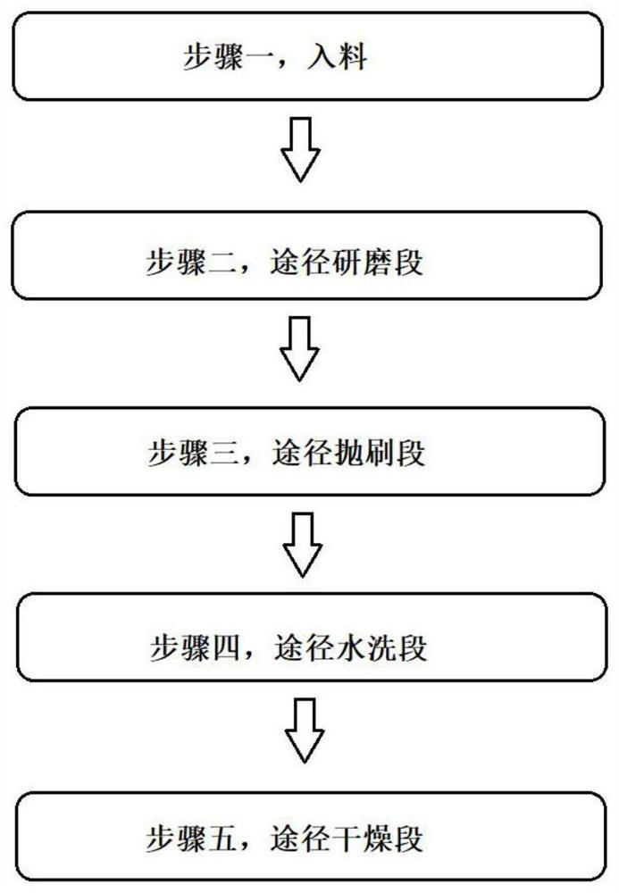
[0033] Specific embodiment 1: see Figure 1 to Figure 4 , a method for treating surface defects of a copper-clad ceramic substrate, comprising the following steps:
[0034] Step 1, the copper-clad ceramic substrate 2 is fed, and conveyed by the belt 1, the transmission speed of the belt 1 is 0.8-1.0m / min, and the brush surface to be thrown is facing upward;
[0035] Step 2, the copper-clad ceramic substrate 2 is ground through the grinding section; the grinding section is provided with a ceramic brush roll 3 and a non-woven brush roll 4; the speed of the brush rolls is 1800-2200 rad / min.
[0036] The mesh number of ceramic brush roller 3 is 400 mesh, and the mesh number of nonwoven brush roller 4 is 400 mesh.
[0037] In the second step, the electric current of the ceramic brush roller is 0.4A-1.4A, and the electric current of the non-woven brush roller is 0.8A-1.8A.
[0038] The thinning amount in step 2 is 8-12 μm;
[0039] Step 3: Brushing the copper-clad ceramic substra...
PUM
 Abstract
Description
Claims
Application Information
 - R&D Engineer
- R&D Manager
- IP Professional
- Industry Leading Data Capabilities
- Powerful AI technology
- Patent DNA Extraction
Browse by: Latest US Patents, China's latest patents, Technical Efficacy Thesaurus, Application Domain, Technology Topic, Popular Technical Reports.
© 2024 PatSnap. All rights reserved.Legal|Privacy policy|Modern Slavery Act Transparency Statement|Sitemap|About US| Contact US: help@patsnap.com


