Spin wave field effect transistor based on carrier regulation and control and preparation method and application thereof
A field effect transistor and spin wave technology, applied in the field of quantum spin wave devices, can solve the problems of unknown cycle characteristics with electric field, very high requirements for preparation process, and difficulty in realizing electric field response, etc., to accelerate the commercialization process and thermal management. Low cost and the effect of reducing replacement cost
- Summary
- Abstract
- Description
- Claims
- Application Information
AI Technical Summary
Problems solved by technology
Method used
Image

Examples
Embodiment 1
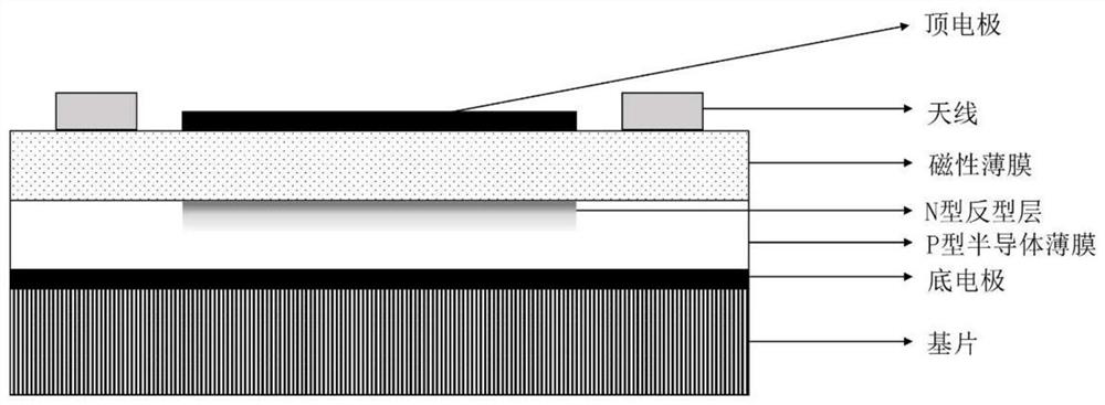
[0038] Such as figure 2 Shown is a side view of the spin wave field effect transistor based on carrier regulation described in this embodiment.
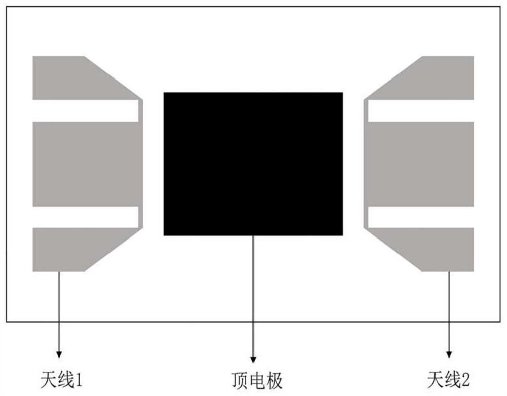
[0039] A spin-wave field effect transistor based on carrier regulation, including a gadolinium gallium garnet (GGG) single crystal substrate, a bottom electrode layer of platinum (Pt), a P-type semiconductor thin film silicon (Si), and a magnetic thin film yttrium iron garnet Stone (YIG), microwave antenna chromium / gold (Cr / Au), and top electrode layer chromium / gold (Cr / Au).
[0040] Apply a positive bias on the top electrode layer to ensure that the electric field strength is greater than 0.02V / nm and less than 0.5V / nm at the same time, and an N-type inversion layer will appear on the upper surface of the P-type semiconductor film, adjusting the spin wave on the lower surface of the magnetic film propagating, the spin wave is regulated by the carrier electrons in the inversion layer.
[0041] The preparation process of the spin w...
Embodiment 2
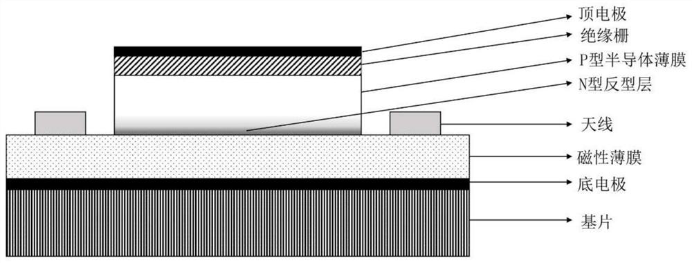
[0049] Such as image 3 Shown is a side view of the spin wave field effect transistor based on carrier regulation described in this embodiment.
[0050] A spin-wave field effect transistor based on carrier regulation, including a gadolinium gallium garnet (GGG) single crystal substrate, a bottom electrode layer of platinum (Pt), a magnetic thin film of yttrium iron garnet (YIG), and a P-type semiconductor thin film Silicon (Si), Insulated Gate Silicon Dioxide (SiO 2 ), microwave antenna chromium / gold (Cr / Au), and top electrode layer chromium / gold (Cr / Au).
[0051] Apply a negative bias voltage on the top electrode layer to ensure that the electric field strength is greater than 0.02V / nm and less than 0.5V / nm at the same time, and an N-type inversion layer will appear on the lower surface of the P-type semiconductor film, adjusting the spin wave on the upper surface of the magnetic film propagating, the spin wave is regulated by the carrier electrons in the inversion layer. ...
Embodiment 3
[0061] A spin-wave field effect transistor based on carrier regulation, including a gadolinium gallium garnet (GGG) single crystal substrate, a bottom electrode layer of platinum (Pt), an N-type semiconductor film of indium tin oxide (ITO), and a magnetic film of yttrium Iron garnet (YIG), microwave antenna chromium / gold (Cr / Au), and top electrode layer chromium / gold (Cr / Au).
[0062] Apply a negative bias voltage on the top electrode layer to ensure that the electric field strength is greater than 0.02V / nm and less than 0.5V / nm at the same time, a P-type inversion layer will appear on the upper surface of the N-type semiconductor film, and the spin wave will be adjusted on the lower surface of the magnetic film. propagating, the spin wave is regulated by the carrier holes in the inversion layer.
PUM
| Property | Measurement | Unit |
|---|---|---|
| thickness | aaaaa | aaaaa |
| thickness | aaaaa | aaaaa |
| thickness | aaaaa | aaaaa |
Abstract
Description
Claims
Application Information
 - R&D
- Intellectual Property
- Life Sciences
- Materials
- Tech Scout
- Unparalleled Data Quality
- Higher Quality Content
- 60% Fewer Hallucinations
Browse by: Latest US Patents, China's latest patents, Technical Efficacy Thesaurus, Application Domain, Technology Topic, Popular Technical Reports.
© 2025 PatSnap. All rights reserved.Legal|Privacy policy|Modern Slavery Act Transparency Statement|Sitemap|About US| Contact US: help@patsnap.com