


Quick Research
Generate reliable direction feasibility study reports for your R&D in just a few steps.

Technical Q&A
Discover and master advanced knowledge NOW. Basics, ideas, possibilities, all at once.

Find Solutions
As an expert in R&D theories, this can generate solutions to your technical problems instantly.

Evaluate Feasibility
Analyze your overall solution with one click, know your potential R&D risks in advance.

Monitor Landscape
Get weekly tech updates, stay abreast of the latest tech innovations and key insights.
Solar blind ultraviolet photoelectric detector and application thereof
A technology of electrical detectors and ultraviolet light, which is applied in the direction of circuits, electrical components, semiconductor devices, etc., can solve the problems of poor spectral selectivity and less spectral selection of detectors, and achieve improved spectral selectivity, high spectral selectivity, and improved stability sexual effect
- Summary
- Abstract
- Description
- Claims
- Application Information
AI Technical Summary
Problems solved by technology
Method used
Image

Examples
Embodiment 1
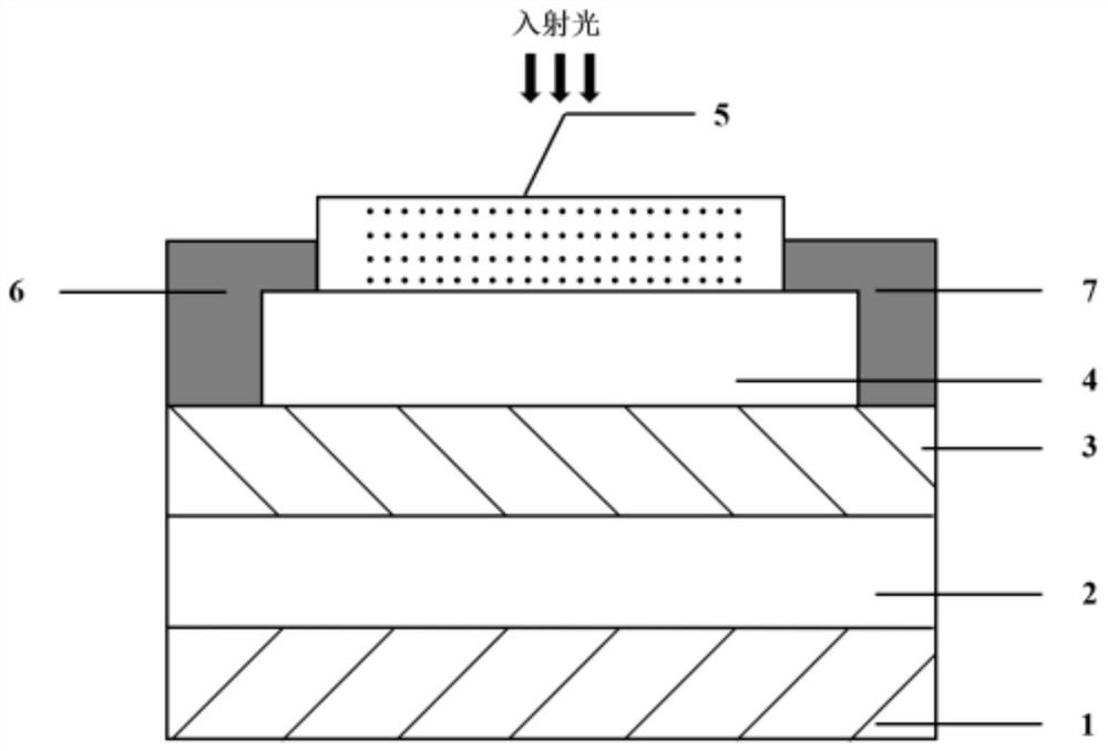
[0045] The sun-blind ultraviolet detector of the present embodiment adopts such as figure 1 Bottom gate structure shown.
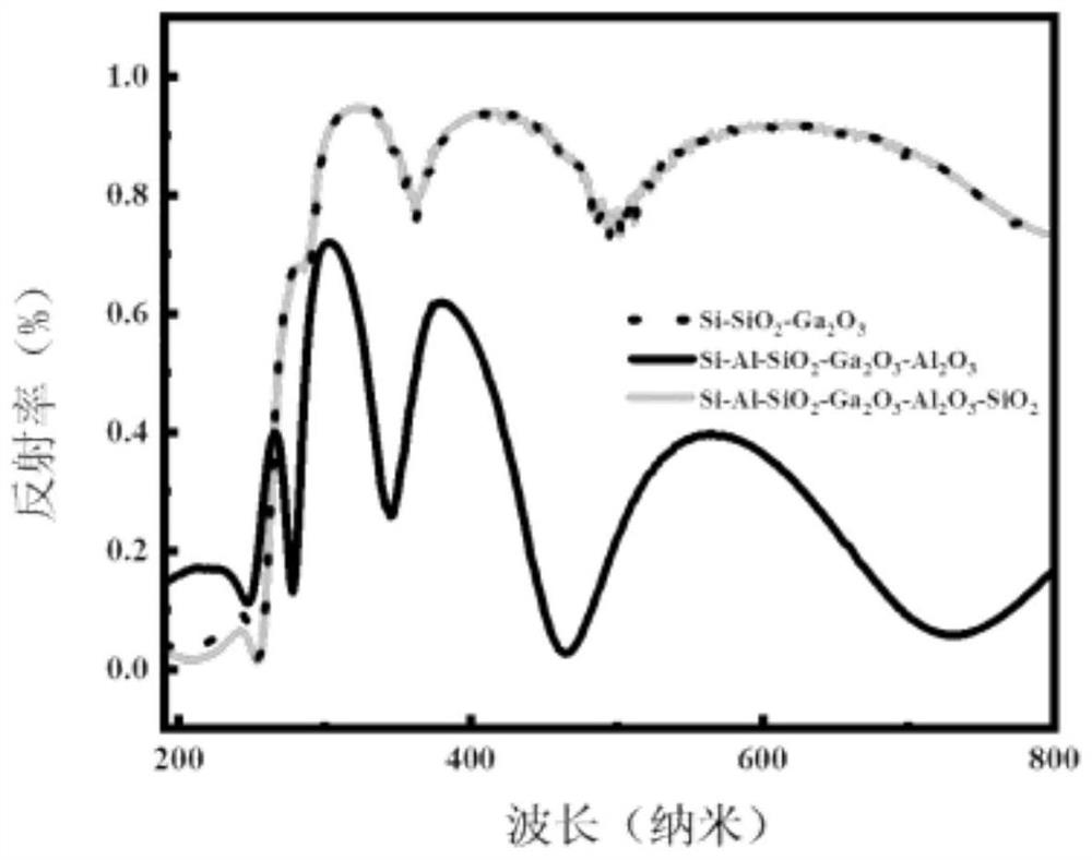
[0046] Substrate 1, gate electrode 2, gate dielectric layer 3, channel layer 4 and cover layer 5 are sequentially made of heavily doped silicon, metal aluminum, silicon oxide, amorphous gallium oxide, aluminum oxide or a stack of aluminum oxide and silicon oxide. layer, the specific film system is Si-Al-SiO 2 -Ga 2 o 3 -Al 2 o 3 (increased anti-reflection layer) and Si-Al-SiO 2 -Ga 2 o 3 -Al 2 o 3 -SiO 2 (anti-reflective layer in laminated form).
[0047] By changing the thickness of different film layers, the reflectance of the film system to light in different bands is simulated by using ellipsometric software, and the reflection gain multiples at 254nm, 320nm and 450nm bands are calculated.
[0048] Finally, the optimal thickness of the film system is obtained respectively, using the Al enhancement layer and the Al 2 o 3 Cover layer: Si(1m...
Embodiment 2
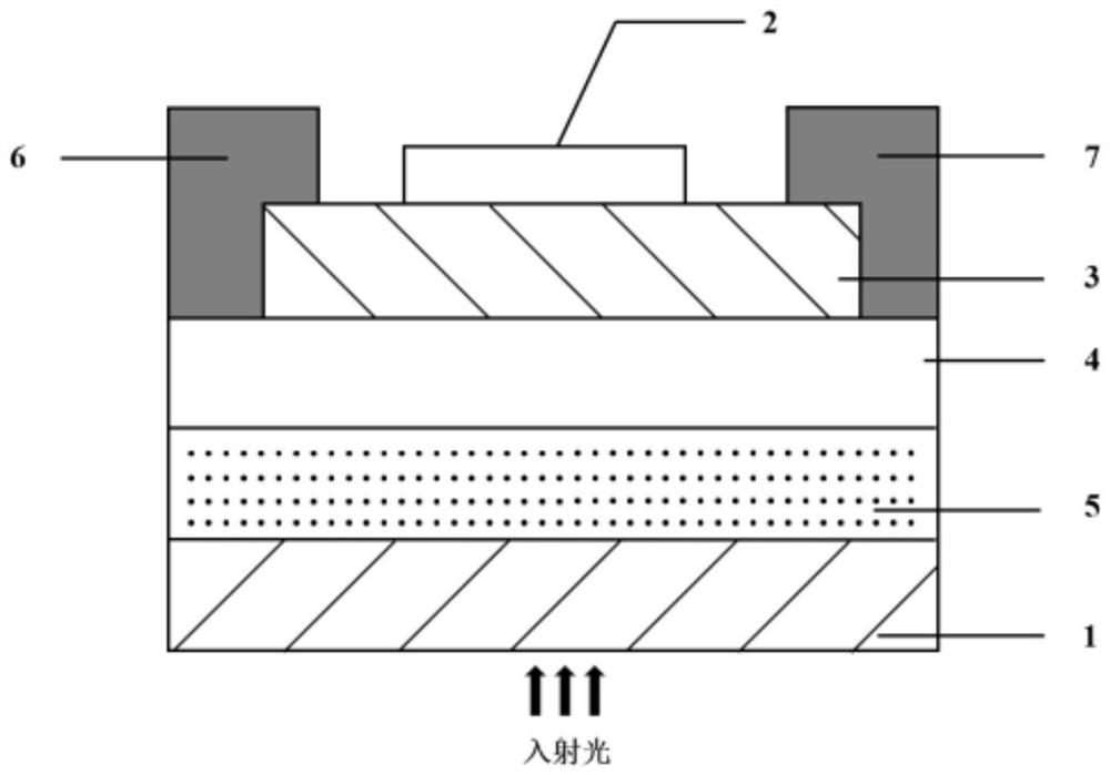
[0057] The sun-blind ultraviolet detector of the present embodiment adopts such as figure 1 Bottom gate structure shown.
[0058] Substrate 1, gate electrode 2, gate dielectric layer 3, channel layer 4, and cover layer 5 are made of heavily doped silicon, metal aluminum, aluminum oxide, amorphous gallium oxide, and aluminum oxide in sequence, and the specific film system is Si-Al -Al 2 o 3 -Ga 2 o 3 -Al 2 o 3 (add anti-reflection layer).
[0059] By changing the thickness of different film layers, the reflectance of the film system to light in different bands is simulated by using ellipsometric software, and the reflection gain multiples at 254nm, 320nm and 450nm bands are calculated.
[0060] The optimal film thickness is Si(1mm)-Al(50nm)-Al 2 o 3 (150nm)-Ga 2 o 3 (190nm)-Al 2 o 3 (20nm). It also includes a comparison film system that does not modify the surface of the channel layer and does not use a metal aluminum layer with an anti-reflection effect, specific...
Embodiment 3
[0069] The sun-blind ultraviolet detector of the present embodiment adopts such as figure 1 Bottom gate structure shown.
[0070] Substrate 1, gate electrode 2, gate dielectric layer 3, channel layer 4, and cover layer 5 are made of heavily doped silicon, metal aluminum, hafnium oxide or stacked layers of silicon oxide and hafnium oxide, amorphous gallium oxide, oxide Lamination of aluminum or aluminum oxide and silicon oxide, the specific film system is Si-Al-HfO 2 -Ga 2 o 3 -Al 2 o 3 (Add anti-reflection layer), Si-Al-HfO 2 -Ga 2 o 3 -SiO 2 -Al 2 o 3 (anti-reflection layer in laminated form) and Si-Al-SiO 2 -HfO 2 -Ga 2 o 3 -SiO 2 -Al 2 o 3 (Gate dielectric layer and anti-reflection layer in stacked form). By changing the thickness of different film layers, the reflectance of the film system to light in different bands is simulated by using ellipsometric software, and the reflection gain multiples at 254nm, 320nm and 450nm bands are calculated. Finally, th...
PUM
| Property | Measurement | Unit |
|---|---|---|
| thickness | aaaaa | aaaaa |
| thickness | aaaaa | aaaaa |
| thickness | aaaaa | aaaaa |
Abstract
Description
Claims
Application Information
 - R&D Engineer
- R&D Manager
- IP Professional
- Industry Leading Data Capabilities
- Powerful AI technology
- Patent DNA Extraction
Browse by: Latest US Patents, China's latest patents, Technical Efficacy Thesaurus, Application Domain, Technology Topic, Popular Technical Reports.
© 2024 PatSnap. All rights reserved.Legal|Privacy policy|Modern Slavery Act Transparency Statement|Sitemap|About US| Contact US: help@patsnap.com