
Schmitt trigger based on GaAs HEMT process

A Schmitt trigger and process technology, applied in the direction of pulse generation, electrical components, and electric pulse generation, to achieve the effects of strong anti-interference and anti-radiation capabilities, small transmission delay, and fast switching speed

Pending Publication Date: 2021-08-06
芜湖麦可威电磁科技有限公司
View PDF0 Cites 0 Cited by
  • Summary
  • Abstract
  • Description
  • Claims
  • Application Information

AI Technical Summary

Problems solved by technology

Although it is not suitable for logic control circuits, when the GaAs process is determined in the integrated circuit, it is also necessary to use the GaAs process to realize some control circuits under certain circumstances. The design of the control circuit must overcome the limitations of the gallium arsenide process. The inherent defects of transistors are used to realize a reliable logic control circuit. Schmitt triggers in the prior art have a wide range of application scenarios, but the Schmitt triggers implemented by GaAs process transistors are not available in the prior art. Based on this, the application provides a Schmitt trigger circuit based on GaAs HEMT technology

Method used


Image

  • Schmitt trigger based on GaAs HEMT process
  • Schmitt trigger based on GaAs HEMT process
  • Schmitt trigger based on GaAs HEMT process

Examples


Embodiment 1

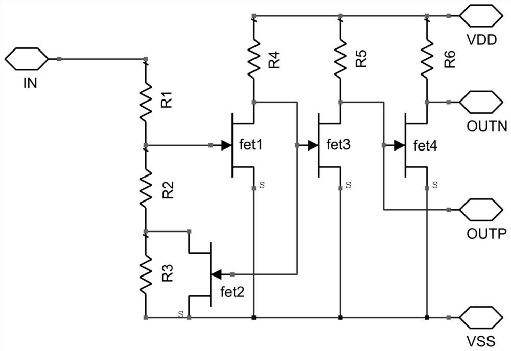
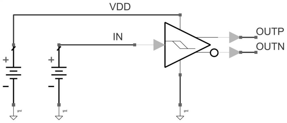
[0022] Embodiment 1: as figure 1 As shown, its circuit structure is specifically: a Schmitt trigger based on GaAs HEMT technology, including field effect transistors fet1, fet2, fet3, and fet4, and field effect transistors fet1, fet2, fet3, and fet4 are all made of GaAs materials. The formed transistor is an enhancement type field effect transistor.

[0023] The Schmitt trigger has an input terminal IN, a positive power supply terminal VDD, a negative power supply terminal VSS, an output non-inverting terminal OUTP, and an output inverting terminal OUTN. The input terminal IN is connected to a resistor R1, and the other end of the resistor R is connected in series with resistors R2 and R3. Then connect the negative terminal VSS of the power supply, the lead terminal between the resistor R1 and the resistor R2 is connected to the gate of the fet1, the drain of the fet1 is connected to the positive terminal VDD of the power supply through the resistor R4; Connect the drain of f...

Embodiment 2

[0032] Embodiment 2: as Figure 4 As shown, the Schmitt trigger in this embodiment is improved on the basis of Embodiment 1. A diode is connected in series between the input terminal IN of the Schmitt trigger in the embodiment and the resistor R1 for voltage reduction, and the input A diode d1 for step-down is connected in series between the terminal IN and the resistor R1. The diode d1 is a single diode or a plurality of diode groups connected in series.

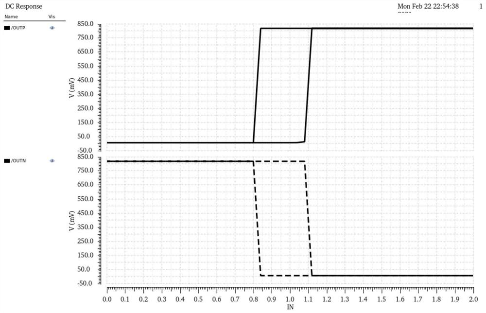
[0033] For some applications with higher voltage (such as 5V-TTL), you can directly divide the voltage with resistors according to the above figure, or you can add diode d1 to step down the voltage as shown in the figure below, and adjust the input logic level threshold to 2V ~ 3V, hysteresis voltage 1V. Although only one diode is shown in the figure, if VSS is powered by a negative voltage, that is, the IN-VSS voltage difference is large, the number of series diodes can be increased to achieve a larger range of level shi...

Embodiment 3

[0034] Embodiment 3: This embodiment is an improvement on the basis of Embodiment 1 or 2, and is mainly applicable to scenarios where low power consumption is required for the Schmitt trigger or the voltage of the power supply VDD-VSS is very high. If the circuit pair requires low power consumption, or the VDD-VSS voltage is very high, the pull-up resistors R4, R5, and R6 need to be large, which will inevitably increase the circuit area. Therefore, D-mode transistors can be used to add resistors to form a constant current. source to limit the operating current while reducing the circuit area. The specific circuit principles include: on the basis of embodiment 1 or 2, adding depletion type field effect transistors dfet1, dfet2, dfet3, such as Figure 5 As shown, dfet1 is set in series between resistor R4 and VDD; dfet2 is set in series between resistor R5 and VDD; dfet3 is set in series between resistor R6 and VDD; VDD is respectively connected to the drain of dfet1, the drain ...


PUM


Abstract

The invention discloses a Schmitt trigger based on a GaAs HEMT process, which comprises field effect transistors fet1, fet2, fet3 and fet4. An input end IN is connected with a resistor R1, the other end of a resistor R is sequentially connected with resistors R2 and R3 in series and then is connected with a negative end VSS of a power supply, a leading-out terminal between the resistor R1 and the resistor R2 is connected with a grid electrode of the fet1, and a drain electrode of the fet1 is connected with a positive end VDD of the power supply through a resistor R4; the positive end of the power supply is connected with the drain electrode of the fet3 through a resistor R5 and is connected with the drain electrode of the fet4 through a resistor R6; the source electrode of the fet1, the source electrode of the fet2, the source electrode of the fet3 and the source electrode of the fet4 are connected with the negative electrode VSS of the power supply; the drain electrode of the fet1 is connected with the grid electrode of the fet3; the drain electrode leading-out terminal of the fet1, which is connected with the grid electrode of the fet4, of the drain electrode of the fet3 is connected to the grid electrode of the fet2, and the drain electrode of the fet2 is connected between the R3 and the R2; the drain electrode leading-out terminal of the fet3 is connected to an output in-phase end OUTP; the drain electrode leading-out terminal of the fet4 is connected to an output inverting end OUTN. The scheme of the invention has the advantages of high switching speed, small transmission delay, interference resistance, continuously adjustable output voltage in a wide range and the like.

Description

technical field [0001] The invention relates to the field of integrated circuit design, in particular to a Schmitt trigger based on GaAs HEMT technology. Background technique [0002] Gallium arsenide (GaAs) is a new generation of wide-bandgap semiconductor materials, belonging to III-V compound semiconductors, which entered the practical stage in 1964. Gallium arsenide can be made into a semi-insulating high-resistance material whose resistivity is more than 3 orders of magnitude higher than that of silicon and germanium, and is used to make integrated circuit substrates, infrared detectors, gamma photon detectors, etc. Because its electron mobility is 5 to 6 times larger than that of silicon, it has been widely used in the manufacture of microwave devices and high-speed digital circuits. Semiconductor devices made of gallium arsenide have the advantages of high frequency, high temperature, low temperature performance, low noise, and strong radiation resistance. There are...

Claims


Application Information

Patent Timeline
Patent Type & Authority Applications(China)
IPC IPC(8): H03K3/3565
CPCH03K3/3565
Inventor 许欢冷益平杨春鹏
Owner 芜湖麦可威电磁科技有限公司
Learn More