Manufacturing method of intelligent full-color toning COB light source

A production method and light source technology, which is applied in the direction of electrical components, circuits, semiconductor devices, etc., can solve problems such as leakage and affecting light output of COB chips, and achieve the effect of reducing glue overflow and avoiding leakage

Active Publication Date: 2021-08-06
ZHUHAI HONGKE OPTOELECTRONICS
View PDF9 Cites 1 Cited by
  • Summary
  • Abstract
  • Description
  • Claims
  • Application Information

AI Technical Summary

Problems solved by technology

[0003] In the process of conventional COB light source processing, there are usually the following technical problems: COB chips are generally bonded to the packaging substrate through die-bonding adhesive during COB packaging, but in the actual dispensing process, it is easy to appear due to excessive dispensing. As a result, the die-bonding glue covers the side of the COB chip, which affects the light output of the COB chip. At the same time, the die-bonding glue is generally a conductive silver glue, and it is prone to leakage.

Method used


Image

  • Manufacturing method of intelligent full-color toning COB light source
  • Manufacturing method of intelligent full-color toning COB light source
  • Manufacturing method of intelligent full-color toning COB light source

Examples


Embodiment 1

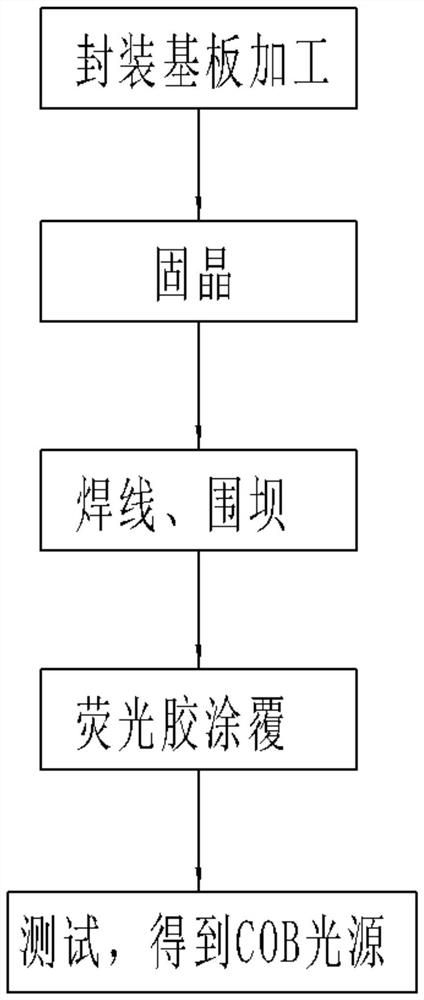
[0058] A method for manufacturing an intelligent full-color toning COB light source, comprising the following steps:

[0059] (1) Prepare the packaging substrate:

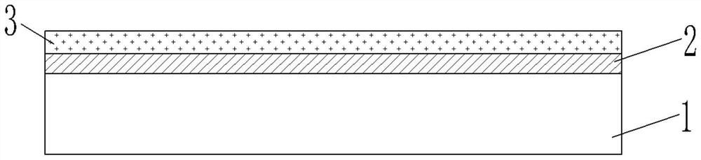
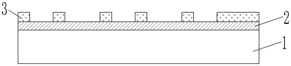
[0060] A. Take the single-sided copper-clad laminate, cut it into a preset size, and set it aside; the single-sided copper-clad laminate includes the single-sided copper-clad laminate substrate 1 and the copper plating layer 2;

[0061] B. Use a brushing machine to remove the oxide film on the surface of the copper clad laminate, coat the positive photoresist 3 on the copper plating layer 2 on the surface of the copper clad laminate, bake and cure, expose the pattern of the solid crystal area through the mask plate, and place it in the developing Develop and etch in the liquid to form several solid crystal regions;

[0062] C. Place the single-sided copper-clad laminate in an ICP etching machine, perform ICP etching on the die-bonding area and form a die-bonding groove, and remove the positive photoresist; the ICP...

Embodiment 2

[0079] A method for manufacturing an intelligent full-color toning COB light source, comprising the following steps:

[0080] (1) Prepare the packaging substrate:

[0081] A. Take the single-sided copper-clad laminate, cut it into a preset size, and set it aside;

[0082] B. Use a brushing machine to remove the oxide film on the surface of the copper-clad laminate, apply a positive photoresist on the copper-plated layer 2 on the surface of the copper-clad laminate, bake and cure, expose the pattern of the crystal-bonding area through the mask plate, and place it in the developer Develop and etch in the middle to form several solid crystal regions;

[0083] C. Place the single-sided copper-clad laminate in an ICP etching machine, perform ICP etching on the die-bonding area and form a die-bonding groove; remove the positive photoresist; the ICP etching depth is a, and the thickness of the COB chip is b , the thickness of copper plating layer 2 is c, then

[0084] c+0.4b=a.

...

Embodiment 3

[0101] A method for manufacturing an intelligent full-color toning COB light source, comprising the following steps:

[0102] (1) Prepare the packaging substrate:

[0103] A. Take the single-sided copper-clad laminate, cut it into preset specifications and sizes, and set aside;

[0104] B. Use a brushing machine to remove the oxide film on the surface of the copper-clad laminate, apply a positive photoresist on the copper-plated layer 2 on the surface of the copper-clad laminate, bake and cure, expose the pattern of the crystal-bonding area through the mask plate, and place it in the developer Develop and etch in the middle to form several solid crystal regions;

[0105] C. Place the single-sided copper-clad laminate in an ICP etching machine, perform ICP etching on the die-bonding area and form a die-bonding groove; remove the positive photoresist; the ICP etching depth is a, and the thickness of the COB chip is b , the thickness of copper plating layer 2 is c, then

[010...


PUM


Abstract

The invention discloses a manufacturing method of an intelligent full-color toning COB light source. The intelligent full-color toning COB light source comprises a packaging substrate, a COB chip and solid crystal glue. When the packaging substrate is prepared, an original solid crystal area is creatively set into a plurality of transverse die bonding grooves and longitudinal die bonding grooves, the sizes of the transverse die bondinggrooves and the longitudinal die bonding grooves are consistent with the sizes of the COB chip needing to be glued, meanwhile, the grooves are formed in the die bonding grooves, and after glue is dispensed in the die bonding grooves subsequently, the die bonding glue can enter the grooves, so that the glue overflowing condition can be reduced to a great extent, the die bonding glue is not prone to covering the side edge of the COB chip during glue joint, and the electric leakage condition is avoided. The COB light source prepared by the invention is high in light emitting efficiency and uniform in light emitting, the side edge of the COB chip is not coated with glue in the preparation process, the die bonding glue does not overflow, and the COB light source is high in yield and reliability, excellent in light emitting effect and higher in practicability.

Description

technical field [0001] The invention relates to the technical field of COB light source processing, in particular to an intelligent full-color color-matching COB light source manufacturing method. Background technique [0002] COB light source is a high-efficiency integrated surface light source technology that directly pastes LED chips on a metal substrate. This technology eliminates the concept of brackets, no electroplating, no reflow soldering, and no SMT process, so the process is reduced by nearly one-third and the cost is also reduced. Saved a third. [0003] In the process of conventional COB light source processing, there are usually the following technical problems: COB chips are generally bonded to the packaging substrate through die-bonding adhesive during COB packaging, but in the actual dispensing process, it is easy to appear due to excessive dispensing. As a result, the die-bonding glue covers the side of the COB chip, which affects the light output of the C...

Claims


Application Information

Patent Timeline
Patent Type & Authority Applications(China)
IPC IPC(8): H01L33/48H01L33/62
CPCH01L33/48H01L33/483H01L33/62H01L2933/0033H01L2933/0066
Inventor 陈秀莲林建辉黄泽语
Owner ZHUHAI HONGKE OPTOELECTRONICS
Why Eureka
Try Eureka