Graphene-based low-altitude airborne infrared remote sensor

A graphene-based, graphene-based technology, applied in sustainable manufacturing/processing, climate sustainability, semiconductor devices, etc., can solve the problems of low absorbance, inability to generate photocurrent, high carrier mobility, etc., and achieve chemical inertness Strong, improve imaging clarity, high sensitivity effect

Active Publication Date: 2021-07-20
ZHEJIANG UNIV
View PDF7 Cites 0 Cited by
  • Summary
  • Abstract
  • Description
  • Claims
  • Application Information

AI Technical Summary

Problems solved by technology

[0003] At present, commercial infrared remote sensing devices are mainly composed of silicon bases. However, due to the extremely shallow transmission depth of infrared light in silicon, the photogenerated carriers are all concentrated on the surface of silicon, but for general junction devices, they have a certain depth. The carrier recombination effect will cause the optical gain of the device to decrease rapidly with the decrease of the incident light wavelength, so silicon-based optoelectronic devices have poor detection ability for infrared rays
Graphene absorbs all wavelengths of light and its carrier mobility is extremely high, so graphene-based infrared optoelectronic devices have attracted the attention of many people; currently, graphene-based infrared optoelectronic devices mainly use Most of them are single-layer or few-layer (less than 5 layers) graphene, but because the absorbance of single-layer and few-layer graphene is very low, it cannot absorb light of sufficient intensity, so it cannot produce effective photocurrent, so most of the current graphite Alkene-based optoelectronic devices mainly use the high carrier mobility of graphene to accelerate the transport of photogenerated carriers generated by semiconductors.

Method used


Image

  • Graphene-based low-altitude airborne infrared remote sensor
  • Graphene-based low-altitude airborne infrared remote sensor
  • Graphene-based low-altitude airborne infrared remote sensor

Examples


Embodiment 1

[0050] Embodiment 1: Preparation of graphene film enhanced by weak coupling

[0051] Graphene oxide is prepared by centrifugal spraying method to prepare nano-thick films. After detaching the nano-film from the substrate, the temperature is raised to 2000 degrees at a rate of 10 degrees Celsius per minute, maintained for 2 hours, and then heated to 2300 degrees Celsius for 4 hours.

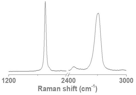
[0052] Such as figure 1 , the measured ID / IG of the graphene film is 0, the AB structure content is 50%, and the graphene structure contains 63 graphene units, and the average number of layers of the graphene units is 2 layers, including several Graphene units composed of graphene sheets and several graphene units composed of more than two layers of graphene sheets in an AB stacking manner, for example, 5 graphene units composed of single-layer graphene sheets and 1 graphene unit composed of 7 layers of graphene A graphene unit composed of sheets in an AB stacking manner.

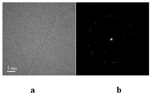
[0053] figure 2 It ...

Embodiment 2

[0059] The graphene film that embodiment 1 prepares is made optoelectronic device according to the following steps:

[0060] 1) First reserve a working window on the Si substrate, plate an insulating layer outside the working window, and then sputter the Pt electrode layer in the insulating layer;

[0061] 2) Spread the graphene film on the working window first, and contact with the electrode layer, drop ethylene glycol on the edge of the graphene film, ethylene glycol penetrates from the edge of the graphene film to the inside, volatilize the solvent, and use the surface of the solvent Tension realizes the tight combination of film and semiconductor;

[0062] (3) Repeat steps 1-2 to prepare an array of windows by photolithography, transfer the film to the windows, and continue to remove the excess parts outside the windows by photolithography. The size of a single window is controlled within 5um, the window spacing is 5um, and the size of the array is 3cm×3cm.

[0063] (4) ...

Embodiment 3

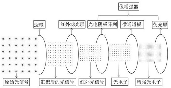
[0084]A layer of Thorlabs infrared filter layer is installed on the back of the lens. This filter layer can filter out light waves with wavelengths other than 750nm-1mm, and the transmittance of light in the range of 750nm-1mm is greater than 90%, so as to eliminate other The impact of light in the wavelength band; it is loaded on the front end of the image intensifier, where the image intensifier contains a photocathode array for photoelectric conversion, a microchannel plate for electron multiplication and a phosphor screen for electron imaging (such as image 3 shown).

[0085] The photocathode units in the photocathode arrays of the remote sensing devices 1 and 2 are 3000×3000 photocathode arrays composed of photocathode units prepared in Example 2 and Comparative Example remote sensing device 1, respectively.

[0086] Such as Figure 4 As shown, when the aircraft flies to 2 kilometers, 4 kilometers, and 6 kilometers away from the ground fire source, three fire sources A,...


PUM

PropertyMeasurementUnit
retention rateaaaaaaaaaa

Abstract

The invention discloses a graphene-based low-altitude airborne infrared remote sensor. The graphene-based low-altitude airborne infrared remote sensor comprises a lens, an infrared filter layer and an image intensifier, the image intensifier comprises a photoelectric cathode array used for realizing photoelectric conversion, a micro-channel plate used for realizing electron multiplication and a fluorescent screen used for electronic imaging, a photoelectric cathode unit in the photoelectric cathode array adopts a photoelectric device composed of a semiconductor and a graphene film, and the graphene film is laid on the semiconductor. The lens gathers external light, the infrared filter layer is used for filtering the gathered light and filtering out light beyond an infrared band, the photoelectric cathode unit performs photoelectric conversion on the filtered light, and imaging is realized on the fluorescent screen after the light is subjected to an electron multiplication effect of the micro-channel plate. According to the infrared remote sensor, the detection height of the remote sensor is greatly improved, and meanwhile, the infrared response sensitivity and the temperature adaptability are also improved.

Description

technical field [0001] The invention relates to a low-altitude airborne infrared remote sensing instrument, in particular to a graphene-based low-altitude airborne infrared remote sensing instrument. Background technique [0002] Remote sensing technology is a technology that collects electromagnetic radiation signals of ground objects from artificial satellites, aircraft or other aircraft. Modern remote sensing technology mainly includes information acquisition, transmission, storage and processing. A complete system that completes the above functions is called a remote sensing system, and its core component is a remote sensor that acquires information. Infrared remote sensing refers to the remote sensing technology in which the working band of the sensor is limited to the infrared band. In the electromagnetic spectrum, the spectral interval with a wavelength range of 0.75-1000 μm is usually called the infrared spectral region. Among them, it is divided into near-infrare...

Claims


Application Information

Patent Timeline
Patent Type & Authority Applications(China)
IPC IPC(8): H01L31/101H01L31/0216H01L31/0232
CPCH01L31/101H01L31/02161H01L31/02325Y02A30/60
Inventor 高超沈颖彭蠡
Owner ZHEJIANG UNIV
Why Eureka
Try Eureka