Ultraviolet light-emitting diode with electron deceleration layer structure

A technology of light-emitting diodes and deceleration layers, which is applied in circuits, electrical components, semiconductor devices, etc., can solve the problems of difficulty in significantly improving UV-LED luminous efficiency, limited effect, and high difficulty in epitaxial growth, so as to improve the uniformity of spatial distribution and increase Efficiency, the effect of reducing electron mobility

Inactive Publication Date: 2021-06-18
SOUTHEAST UNIV
View PDF9 Cites 2 Cited by
  • Summary
  • Abstract
  • Description
  • Claims
  • Application Information

AI Technical Summary

Problems solved by technology

However, the use of this technology not only requires high difficulty in epitaxial growth, but also has limited effects, which is not enough to completely prevent the leakage of electrons to the p-type region, and it is difficult to significantly improve the luminous efficiency of UV-LEDs.

Method used


Image

  • Ultraviolet light-emitting diode with electron deceleration layer structure
  • Ultraviolet light-emitting diode with electron deceleration layer structure

Examples


Embodiment Construction

[0013] The present invention will be further explained below in conjunction with the accompanying drawings.

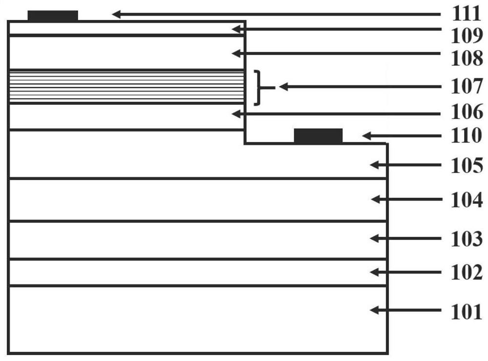
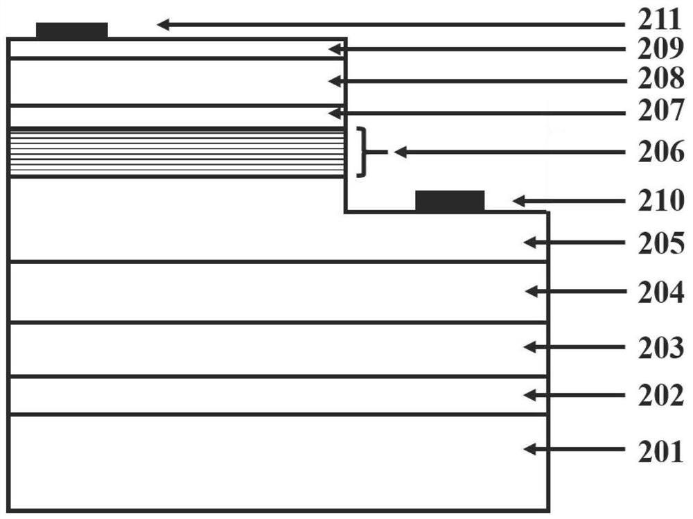
[0014] Such as figure 1 As shown, an ultraviolet light-emitting diode with an electron deceleration layer structure includes a substrate 101, an AlN nucleation layer 102, an AlN buffer layer 103, an undoped AlGaN buffer layer 104, and an n-type AlGaN layer 105 arranged in sequence from bottom to top. , B(Al, Ga)N electron deceleration layer 106, Al x Ga 1-x N / Al y Ga 1-y N multi-quantum well active region 107, p-type AlGaN layer 108 and p-type GaN ohmic contact layer 109, and n-type ohmic electrode 110 set on n-type AlGaN layer 105 and p-type GaN ohmic contact layer 109 set on the p type ohmic electrode 111, where 0<x<y<1.

[0015] The B(Al, Ga)N electron deceleration layer 106 is composed of any one of undoped or n-type doped BAlN, BGaN or BAlGaN layers, and its forbidden band width is always greater than the forbidden band width of the n-type AlGaN layer 105, ...


PUM

PropertyMeasurementUnit
Thicknessaaaaaaaaaa
Thicknessaaaaaaaaaa
Thicknessaaaaaaaaaa

Abstract

The invention discloses an ultraviolet light-emitting diode with an electron deceleration layer structure. The light-emitting diode sequentially comprises a substrate, an AlN nucleating layer, an AlN buffer layer, a non-doped AlGaN buffer layer, an n-type AlGaN layer, a B(Al, Ga)N electron deceleration layer, an Al<x>Ga<1-x>N / Al<y>Ga<1-y>N multi-quantum well active region, a p-type AlGaN layer and a p-type GaN ohmic contact layer from bottom to top. Compared with the Al<x>Ga<1-x>N / Al<y>Ga<1-y>N heterojunction, the B(Al, Ga)N / AlGaN heterojunction has a larger conduction band offset and valence band offset ratio, so that the rate of electrons entering the active region from the n-type region can be limited more effectively. Secondly, a traditional p-type doped electron barrier layer is removed, the efficiency of hole injection into an active region can be improved, and the radiation recombination efficiency of electron holes in the active region is improved. Besides, polarized charges can be generated at the two ends of the B(Al, Ga)N electron deceleration layer, a polarized electric field with the same electron migration direction can be formed, and the migration rate of electrons entering an active region from an n-type region can be reduced, so that the electron capture efficiency of the quantum well is improved, the radiation recombination probability of the electrons and holes in the quantum well is increased, and the light emitting efficiency of the UV-LED is improved.

Description

technical field [0001] The invention relates to the technical field of semiconductor optoelectronic materials and device manufacturing, in particular to an ultraviolet light emitting diode (UV-LED) with an electron deceleration layer structure. Background technique [0002] At present, the luminous efficiency of AlGaN-based UV-LED devices is still very low compared with GaN-based blue LEDs, especially in the deep ultraviolet band, and the external quantum efficiency of devices is often lower than 10%. The main reasons for this phenomenon include the low internal quantum efficiency of AlGaN-based UV-LEDs and the high material defect density in AlGaN materials. Among them, the low internal quantum efficiency is mainly related to the lower electron capture efficiency and lower hole injection efficiency in the active region of the UV-LED, making it easy for electrons to escape the shackles of the quantum well and leak into the p-type region and the holes. Perform nonradiative r...

Claims


Application Information

Patent Timeline
IPC IPC(8): H01L33/14H01L33/06
CPCH01L33/14H01L33/145H01L33/06
Inventor 张雄范艾杰胡国华崔一平
Owner SOUTHEAST UNIV
Why Eureka
Try Eureka