Photovoltaic module for improving photoelectric conversion efficiency and preparation method thereof
A technology of photoelectric conversion efficiency and photovoltaic modules, applied in photovoltaic power generation, electrical components, circuits, etc., can solve the problems of low photoelectric conversion efficiency of photovoltaic cells, high temperature of photovoltaic cells, and damage of photovoltaic cells, etc., to improve light conversion Efficiency, increased refractive index, heat reduction effect
- Summary
- Abstract
- Description
- Claims
- Application Information
AI Technical Summary
Problems solved by technology
Method used
Image
Examples
Embodiment 1
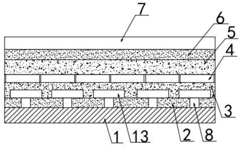
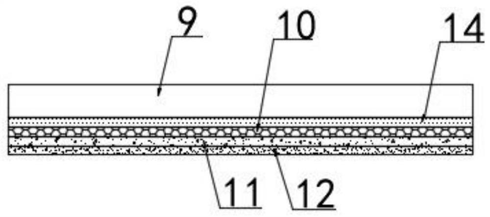
[0028] see Figure 1-2 , the present invention provides a photovoltaic module that improves photoelectric conversion efficiency, and the photovoltaic module includes a backplane 1, a first EVA packaging adhesive layer 2, a thermally conductive packaging adhesive layer 3, a photovoltaic cell sheet layer 4, The heat-insulating packaging adhesive layer 5, the second EVA packaging adhesive layer 6 and the tempered glass cover plate 7, the upper end of the back plate 1 is evenly spaced with several bumps 8, and the upper end of the bumps 8 runs through the first EVA packaging Adhesive layer 2, and embedded in the thermally conductive packaging adhesive layer 3, one end of the bump 3 located inside the thermally conductive packaging adhesive layer 3 is fixed with a heat absorbing plate 13, and the tempered glass cover plate 7 includes a glass substrate 9, The glass substrate 9 is provided with an ultraviolet light absorbing layer 14 , a niobium pentoxide layer 10 , an AZO layer 11 a...
Embodiment 2
[0043] Different from Example 2, the thickness of the glass substrate 9 is 800 microns, the thickness of the niobium pentoxide 10 is 100 nanometers, the thickness of the AZO layer 11 is 100 nanometers, and the thickness of the silver layer 12 is 100 nanometers. The thickness of the ultraviolet absorbing layer 14 is 90 nanometers.
Embodiment 3
[0045] Different from Example 1-2, the thickness of the glass substrate 9 is 800 microns, the thickness of the niobium pentoxide 10 is 120 nanometers, the thickness of the AZO layer 11 is 120 nanometers, and the silver layer 12 The thickness of the ultraviolet light absorbing layer 14 is 150 nanometers.
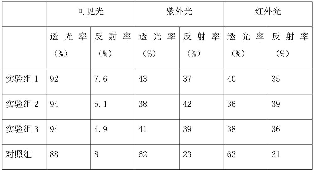
[0046] The tempered glass cover plates of the photovoltaic modules produced in Example 1, Example 2 and Example 3 were respectively selected as the experimental group 1, the experimental group 2 and the experimental group 3, and the tempered glass cover plates of the traditional photovoltaic components were selected as the control group, respectively. The transmittance and reflectance of each group of photovoltaic modules to visible light, ultraviolet light and infrared light were measured, and the measurement results are shown in Table 1:
[0047]
[0048] Table I
[0049] After several experiments, it can be concluded that the tempered glass cover plate of the photovolt...
PUM
| Property | Measurement | Unit |
|---|---|---|
| Thickness | aaaaa | aaaaa |
| Thickness | aaaaa | aaaaa |
| Thickness | aaaaa | aaaaa |
Abstract
Description
Claims
Application Information
 - R&D
- Intellectual Property
- Life Sciences
- Materials
- Tech Scout
- Unparalleled Data Quality
- Higher Quality Content
- 60% Fewer Hallucinations
Browse by: Latest US Patents, China's latest patents, Technical Efficacy Thesaurus, Application Domain, Technology Topic, Popular Technical Reports.
© 2025 PatSnap. All rights reserved.Legal|Privacy policy|Modern Slavery Act Transparency Statement|Sitemap|About US| Contact US: help@patsnap.com


