Circuit board, circuit board via hole optimization method, electronic equipment and storage medium

An optimization method and circuit board technology, applied in printed circuits, printed circuits, printed circuit components, etc., can solve problems such as discontinuous impedance of multi-layer PCB vias

Active Publication Date: 2021-06-01
合肥移瑞通信技术有限公司
View PDF9 Cites 2 Cited by
  • Summary
  • Abstract
  • Description
  • Claims
  • Application Information

AI Technical Summary

Problems solved by technology

[0005] The purpose of the embodiments of the present application is to provide a circuit board via hole optimization method and a circuit board to improve the problem of discontinuous impedance of multi-layer PCB via holes in the prior art, and at the same time, ensure the strength of the PCB without increasing the PCB manufacturing process , reduces manufacturing cost, and does not take up too much PCB layout space

Method used


Image

  • Circuit board, circuit board via hole optimization method, electronic equipment and storage medium
  • Circuit board, circuit board via hole optimization method, electronic equipment and storage medium
  • Circuit board, circuit board via hole optimization method, electronic equipment and storage medium

Examples


Embodiment Construction

[0026] In order to make the purpose, technical solution and advantages of the present application clearer, the present application will be further described in detail below in conjunction with the accompanying drawings and embodiments. It should be understood that the specific embodiments described here are only used to explain the present application, and are not intended to limit the present application.

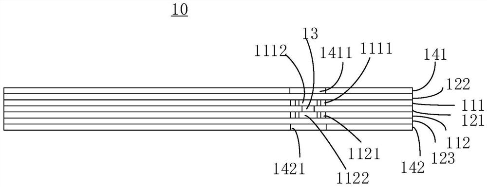
[0027] see figure 1 , an embodiment of the present application provides a circuit board 10 . In this embodiment, the circuit board 10 includes a first circuit layer 111 and a second circuit layer 112 , a first dielectric layer 121 , via holes 13 , a second dielectric layer 122 and a first ground layer 141 .

[0028] The first circuit layer 111 and the second circuit layer 112 respectively have signal circuits. The first circuit layer 111 and the second circuit layer 112 can be formed by using conductive layers such as copper and tungsten through exposure, development, et...


PUM


Abstract

The invention provides a circuit board and a circuit board via hole optimization method. The circuit board comprises: a first circuit layer and a second circuit layer; a first dielectric layer, which is arranged between the first circuit layer and the second circuit layer; a via hole, which penetrates through the first dielectric layer and is electrically connected with the first circuit layer and the second circuit layer, wherein a first anti-bonding pad is arranged around one end, close to the first circuit layer, of the via hole; a second dielectric layer, which is arranged on one side, far away from the second circuit layer, of the first circuit layer; and a first grounding layer, which is arranged on the side, away from the first circuit layer, of the second dielectric layer, wherein a first opening is formed in the area, corresponding to the first anti-bonding pad, of the first grounding layer. According to the invention, the opening is formed in the area, corresponding to the anti-bonding pad, of the grounding layer, so stray capacitance can be prevented from being formed between the grounding layer and the via hole, and the problem that the impedance of via holes in the multi-layer PCB is discontinuous is solved to a certain degree; and meanwhile, the strength of the PCB is guaranteed, manufacturing cost is reduced, and excessive PCB layout space is not occupied.

Description

technical field [0001] The present application relates to the field of printed circuit boards, in particular, to a circuit board and a method for optimizing circuit board vias. Background technique [0002] At present, electronic devices such as mobile phones and notebooks, communication modules, and electronic components such as memory sticks usually use a multilayer PCB (Printed Circuit Board, printed circuit board). In a multi-layer PCB, in order to achieve signal communication between different layers, vias are usually provided. In the high-frequency field, via stubs will cause via impedance discontinuity, or lead to parasitic capacitance or resistance, which will seriously affect the transmission of high-speed signals, cause signal integrity problems, and also cause reflections on the radio frequency link question. [0003] With the improvement of communication bandwidth and data transmission rate in the 5G era, the radio frequency has been increased to the millimeter...

Claims


Application Information

Patent Timeline
Patent Type & Authority Applications(China)
IPC IPC(8): H05K1/02H05K1/11H05K3/42
CPCH05K1/115H05K1/0298H05K3/42H05K2201/095H05K2203/0554
Inventor 徐鹏举张栋郑雷
Owner 合肥移瑞通信技术有限公司
Why Eureka
Try Eureka