A kind of nano-wafer product nitrogen protection cleaning method

A nitrogen protection, nanocrystalline technology, applied in cleaning methods and utensils, cleaning methods using liquids, chemical instruments and methods, etc., can solve problems such as inability to clean nano-wafers, increase the effective spray radius, and improve the spray range. , use flexible effects

Active Publication Date: 2022-07-15
ULTRON SEMICON (SHANGHAI) CO LTD
View PDF7 Cites 0 Cited by
  • Summary
  • Abstract
  • Description
  • Claims
  • Application Information

AI Technical Summary

Problems solved by technology

Storage products such as DRAM NAND and other related structures have different metallization microstructures and high aspect ratio pattern distribution. If the general cleaning method is used, the surface of the nanowafer cannot be cleaned well due to the accumulation of liquid particles. Cleaning is a problem that needs to be solved urgently

Method used


Image

  • A kind of nano-wafer product nitrogen protection cleaning method
  • A kind of nano-wafer product nitrogen protection cleaning method
  • A kind of nano-wafer product nitrogen protection cleaning method

Examples


Embodiment 1

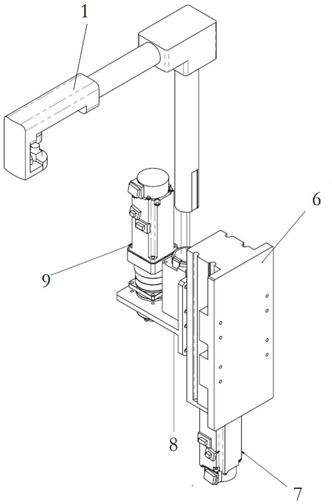
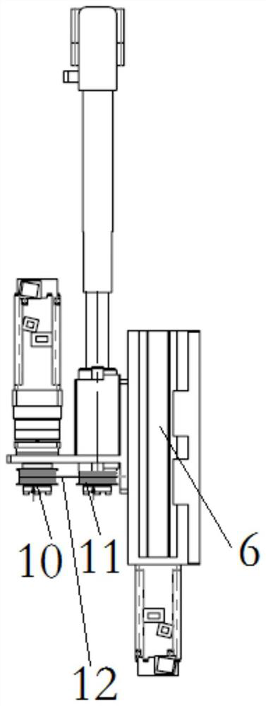
[0033] This embodiment provides a nitrogen protection cleaning device for nano-wafer products, including a wafer carrying mechanism and a wafer cleaning mechanism. Among them, the wafer carrier mechanism is used to place the wafer, and the wafer can be fixed on the upper surface of the wafer carrier mechanism and rotated under the drive of the wafer carrier mechanism. The wafer carrier mechanism can be formed by various structures, for example, The wafer is adsorbed on the surface of the wafer carrier by Bernoulli. This part of the structure can be rotated by those skilled in the art according to the needs of use, and will not be repeated here.

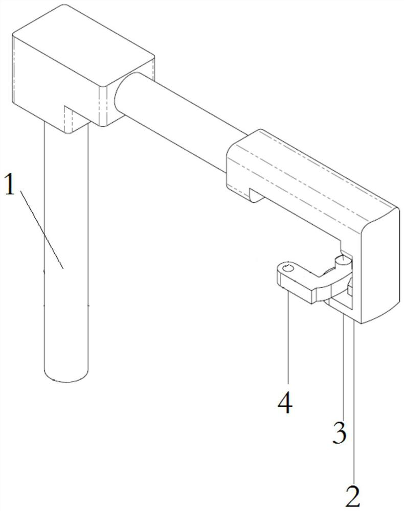
[0034] The wafer cleaning mechanism includes a drive mechanism, a cleaning housing 1, a liquid cleaning nozzle 3, an atomizing cleaning nozzle 2, a nitrogen gas nozzle 4 and an ultrasonic oscillator 5. One end of the cleaning housing 1 is set at one end of the wafer carrying mechanism, and the cleaning housing The body 1 is connected ...

Embodiment 2

[0039] This embodiment provides a nitrogen protection cleaning method for nano-wafer products, which includes the following steps:

[0040] Step 1. Move the liquid cleaning nozzle 3, the atomizing cleaning nozzle 2, and the nitrogen gas nozzle 4 to the top of the wafer, and adjust the distance between the atomizing cleaning nozzle 2 and the wafer to be 14-30 mm; atomization cleaning The distance between the showerhead 2 and the wafer decreases as the aperture of the wafer surface decreases;

[0041] In step 2, the wafer carrying mechanism drives the wafer to rotate, the external air source of the nitrogen nozzle 4 supplies air, blows nitrogen to the surface of the wafer, and turns on the liquid cleaning nozzle 3 and the atomizing cleaning nozzle 2 in turn to supply air to the surface of the wafer. The surface is sprayed with cleaning liquid to clean the surface of the wafer;

[0042] Step 3: After the cleaning is completed, the atomizing cleaning nozzle 2, the liquid cleaning...


PUM


Abstract

The invention discloses a nitrogen protection and cleaning method for nano-wafer products, comprising the following steps: Step 1. Move a liquid cleaning nozzle, an atomizing cleaning nozzle and a nitrogen nozzle to the top of the wafer, and adjust the atomizing cleaning nozzle and the crystal The distance between the wafers is 14-30 mm; in step 2, the wafer carrier mechanism drives the wafer to rotate, the external air source of the nitrogen nozzle supplies air, blows nitrogen to the surface of the wafer, and turns on the liquid cleaning nozzle and mist in turn. The cleaning nozzle sprays the cleaning liquid on the surface of the wafer to clean the surface of the wafer; Step 3: After the cleaning is completed, the atomizing cleaning nozzle, the liquid cleaning nozzle and the nitrogen nozzle are closed in turn, and the positive Move up. The invention adopts nitrogen blowing to form a gas protective film on the surface of the mist water, maintain the surface energy of the liquid, prevent the agglomeration of droplet molecules, and ensure the cleaning effect of the nano-wafer.

Description

technical field [0001] The invention belongs to the technical field of semiconductor cleaning equipment, and particularly relates to a nitrogen protection cleaning method for nano-wafer products. Background technique [0002] In the field of semiconductor cleaning, for high-end wafer products, such as related wafer products involving logic integrated circuits, storage, power devices and other products, in the manufacturing process, through various complex lithography, wet method, deposition, However, after each stage of the process, it needs to be processed by a cleaning process to ensure the accuracy and reproducibility of the subsequent process. [0003] Especially for the wafer cleaning wet process that requires 65-14nm pitch, and the wafer products whose size is below 14nm and extends to 5nm pitch, under the effect of the size effect, the core problem of the wafer wet process is that the liquid remains in the nanometer. in the microstructure of the wafer. Storage produ...

Claims


Application Information

Patent Timeline
Patent Type & Authority Patents(China)
IPC IPC(8): B08B3/02B08B3/10B08B3/12B08B3/08B08B13/00H01L21/02H01L21/67
CPCB08B3/022B08B3/10B08B3/123B08B3/08B08B13/00H01L21/02041H01L21/67051
Inventor 邓信甫张先明刘大威陈丁堃
Owner ULTRON SEMICON (SHANGHAI) CO LTD
Why Eureka
Try Eureka