Staggered wafer surface wet cleaning system and method

A wet cleaning, staggered technology, applied in cleaning methods and utensils, cleaning methods using liquids, chemical instruments and methods, etc., can solve problems such as inability to clean nano-wafers, increase the effective spray radius, improve spray Range, use of flexible effects

Active Publication Date: 2021-05-07
PNC PROCESS SYSTEMS CO LTD +1
View PDF11 Cites 2 Cited by
  • Summary
  • Abstract
  • Description
  • Claims
  • Application Information

AI Technical Summary

Problems solved by technology

Storage products such as DRAM NAND and other related structures have different metallization microstructures and high aspect ratio pattern distributions. If the general cleaning method is used, the surface of the nanowafer cannot be well cleaned due to the accumulation of liquid particles. Cleaning is a problem that needs to be solved urgently

Method used


Image

  • Staggered wafer surface wet cleaning system and method
  • Staggered wafer surface wet cleaning system and method
  • Staggered wafer surface wet cleaning system and method

Examples


Embodiment 1

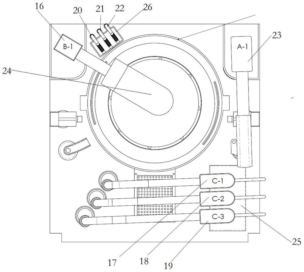
[0051] This embodiment provides a staggered wafer surface wet cleaning system, which is characterized in that it includes a wafer carrying mechanism and a wafer cleaning mechanism, the wafer carrying mechanism is used to place wafers, and the wafers are fixed Rotate on the surface of the wafer carrying mechanism and driven by the wafer carrying mechanism; the wafer cleaning mechanism includes a first cleaning mechanism 23, a second cleaning mechanism 24, a third cleaning mechanism 25 and a fourth cleaning mechanism 26, so The first cleaning mechanism 23 , the second cleaning mechanism 24 , the third cleaning mechanism 25 , and the fourth cleaning mechanism 26 are all arranged outside the wafer carrying mechanism for cleaning the surface of the wafer.

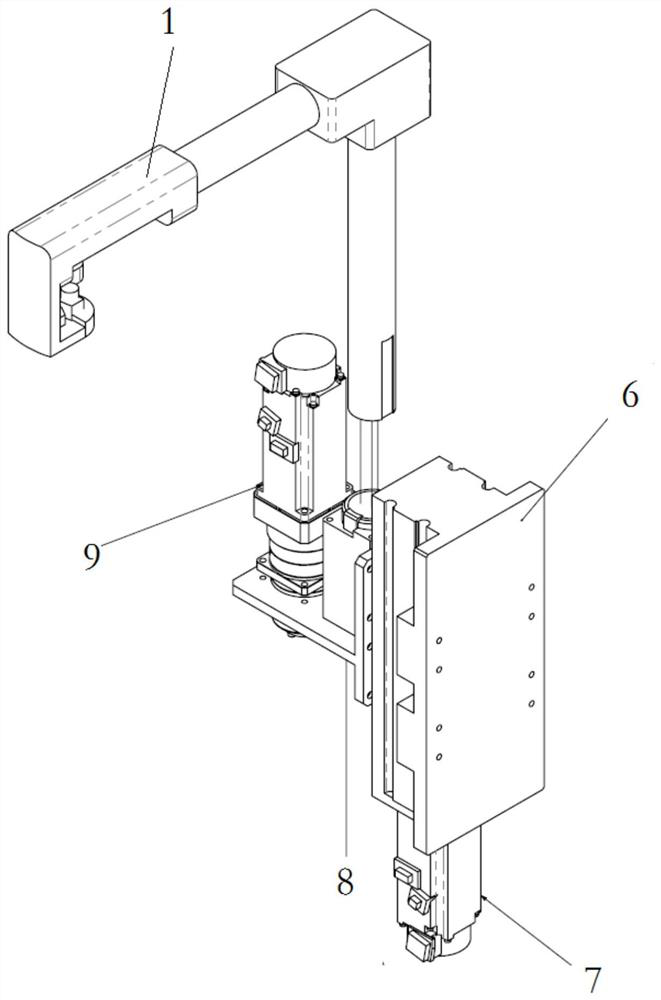
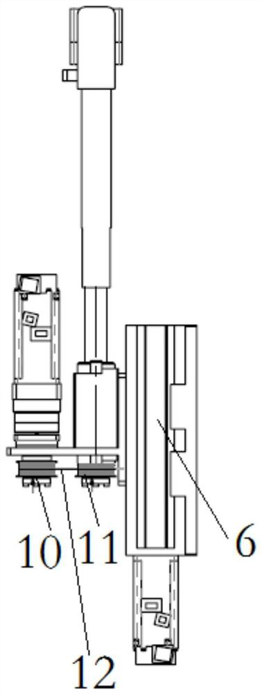
[0052] The first cleaning mechanism 23 includes a driving mechanism, a cleaning housing 1, a liquid cleaning nozzle 3, an atomized cleaning nozzle 2, a nitrogen gas nozzle 4, and an ultrasonic vibrating plate 5. One end of the cl...

Embodiment 2

[0061] This embodiment provides a method for staggered wafer surface wet cleaning, comprising the following steps:

[0062] Step 1, the third cleaning mechanism 25 moves to the top of the wafer, the wafer carrying mechanism drives the wafer to rotate, the third cleaning mechanism 25 sprays hydrofluoric acid solution on the surface of the wafer, after the cleaning is completed, the third The cleaning mechanism 25 drives the third cleaning mechanism 25 away from the wafer;

[0063] Step 2, the fourth cleaning mechanism 26 sprays ultrapure water on the surface of the wafer, and the wafer carrying mechanism stops rotating after the spraying is completed;

[0064] Step 3, the wafer carrying mechanism drives the wafer to rotate at a high speed for 5-10 seconds and then stops to complete the drying of the wafer;

[0065] Step 4, the wafer carrying mechanism drives the wafer to rotate, the fourth cleaning mechanism 26 sprays nitrogen to the surface of the wafer, and the wafer carryin...


PUM


Abstract

The invention discloses a staggered wafer surface wet cleaning system and method. The cleaning system comprises a wafer bearing mechanism and a wafer cleaning mechanism, wherein the wafer bearing mechanism is used for placing a wafer, and the wafer is fixed on the surface of the wafer bearing mechanism and driven by the wafer bearing mechanism to rotate; and the wafer cleaning mechanism comprises a first cleaning mechanism, a second cleaning mechanism, a third cleaning mechanism and a fourth cleaning mechanism, and the first cleaning mechanism, the second cleaning mechanism, the third cleaning mechanism and the fourth cleaning mechanism are all arranged on the outer side of the wafer bearing mechanism and used for cleaning the surfaces of the wafer. According to the invention, multiple cleaning solutions are adopted for staggered cleaning, all cleaning procedures do not interfere with one another, the cleaning quality of the surface of the wafer is improved, and the cleaning effect of the wafer is guaranteed.

Description

technical field [0001] The invention belongs to the technical field of semiconductor wet cleaning equipment, and in particular relates to an interlaced wafer surface wet cleaning system and a cleaning method. Background technique [0002] In the field of semiconductor cleaning, for high-end wafer products, such as related wafer products involving logic integrated circuits, storage, power devices and other products, in the process of manufacturing, through various complex photolithography, wet, deposition, Oxidation and other related processes are processed. However, after each process is completed, it needs to be processed by a cleaning process to ensure the accuracy and reproducibility of subsequent processes. [0003] Especially for the wafer cleaning wet process required by 65-14nm pitch, and the wafer products whose size is below 14nm and extended to 5nm pitch, under the effect of size effect, the core problem of wafer wet process is that the liquid remains in the nanome...

Claims


Application Information

Patent Timeline
Patent Type & Authority Applications(China)
IPC IPC(8): H01L21/67H01L21/02B08B3/02B08B13/00
CPCH01L21/67051H01L21/67253H01L21/02057B08B3/022B08B13/00
Inventor 邓信甫刘大威方超陈丁堃
Owner PNC PROCESS SYSTEMS CO LTD
Why Eureka
Try Eureka