Alkali polishing device and polishing process for crystalline silicon wafer

A technology of polishing device and silicon chip alkali, which is applied in the direction of grinding drive device, grinding/polishing equipment, surface polishing machine tool, etc., can solve the problems of wear and tear on the lower surface of crystal silicon chip, deposition, and flat surface unevenness, and achieve Avoid turning or moving, avoid mechanical damage, improve the effect of polishing effect

Active Publication Date: 2022-05-17
武汉风帆电化科技股份有限公司
View PDF14 Cites 0 Cited by
  • Summary
  • Abstract
  • Description
  • Claims
  • Application Information

AI Technical Summary

Problems solved by technology

[0005] 1. When the crystal silicon wafer is processed by the polishing mold, a large number of fine particles will be produced, which will remain between the lower surface of the crystal silicon wafer and the flat plate, which will not only cause the silicon wafer to fail to maintain its level, but also wear the lower surface of the crystal silicon wafer. The surface of the crystal silicon wafer will have a negative impact on the overall stability; and the polishing liquid will be deposited in the groove, which may cause etching on the lower surface of the crystal silicon wafer and have a negative impact
[0006] 2. The cr

Method used


Image

  • Alkali polishing device and polishing process for crystalline silicon wafer
  • Alkali polishing device and polishing process for crystalline silicon wafer
  • Alkali polishing device and polishing process for crystalline silicon wafer

Examples


Example Embodiment

[0033] The following will be combined with embodiments of the present invention, the technical solution in the embodiment of the present invention is clearly and completely described, it is clear that the embodiments described are only a part of the embodiment of the present invention, not all embodiments. Based on embodiments in the present invention, all other embodiments obtained by those of ordinary skill in the art without making creative work, are within the scope of protection of the present invention.

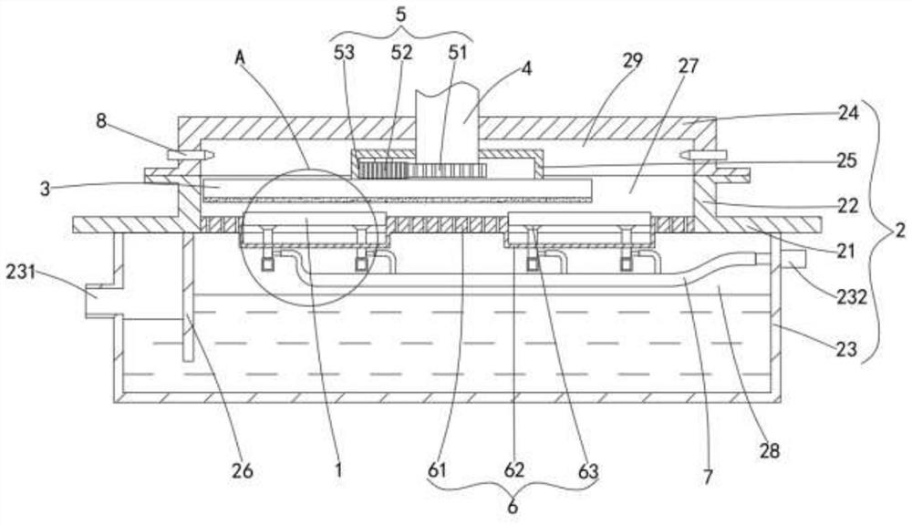
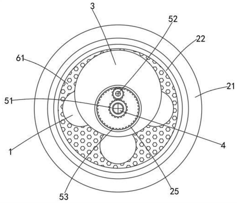
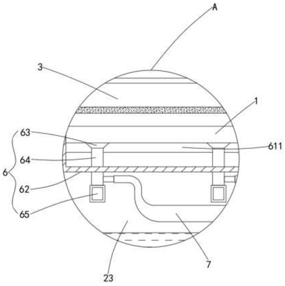
[0034] as Figure 1 As shown, a crystalline silicon wafer alkali polishing apparatus of the present invention, comprising a workpiece 1, further comprising a device body 2, a polishing die 3, a hinge 4, a transmission mechanism 5, a fixed assembly 6, a suction pipe 7 and several nozzles 8.

[0035] Wherein, the apparatus body 2 includes a platform 21, a first cylinder 22, a second cylinder 23 and a first cylinder head 24, a horizontal setting of platform 21.

[0036] The fi...


PUM


Abstract

The invention proposes a crystalline silicon wafer alkali polishing device and a polishing process, including a main body of equipment, a polishing mold, a fixed assembly and a plurality of nozzles, the polishing mold can move along the vertical direction to contact the upper surface of the workpiece, and the polishing mold is supplied by an external The driving device drives and rotates clockwise or counterclockwise around the plumb line, or rotates clockwise or counterclockwise axially around the plumb line to polish the upper surface of the workpiece. The fixed component can make the first cavity body and the third cavity are always in communication, several nozzles are fixedly arranged on the inner peripheral wall of the first cylinder head, and the tail end of the nozzle is fixedly connected with the external source conveying mechanism. When the polishing mold polishes the upper surface of the workpiece, the nozzles will The polishing liquid is continuously input into the second cavity; during the polishing process, the polishing liquid is continuously input through the nozzle, so that there is always a polishing liquid on the upper surface of the workpiece, which improves the polishing effect and avoids mechanical damage caused by the polishing mold to the upper surface of the workpiece.

Description

technical field [0001] The invention relates to the technical field of silicon wafer polishing, in particular to a crystal silicon wafer alkali polishing device and a polishing process. Background technique [0002] Crystalline silicon wafers are important components used in the field of solar photovoltaic power generation. [0003] At present, the traditional crystal silicon wafer polishing process usually uses a large amount of hydrofluoric acid and nitric acid, causing serious pollution and high processing costs; and the traditional acid polishing process has poor stability, and the photoelectric conversion efficiency of the polished silicon wafer is low. Therefore, it is urgent to design a new crystal silicon wafer polishing process. [0004] At the same time, the polishing equipment used in the traditional process generally has the following problems: [0005] 1. When the crystal silicon wafer is processed by the polishing mold, a large number of fine particles will b...

Claims


Application Information

Patent Timeline
IPC IPC(8): B24B29/02B24B27/00B24B41/06B24B47/00B24B47/12B24B57/02H01L21/02H01L21/67
CPCB24B29/02B24B27/0023B24B41/068B24B47/12B24B57/02B24B47/00H01L21/02013H01L21/67092H01L21/67017Y02P70/50
Inventor 张红利罗江李雪芬王池李锋清李杨袁震芹虢世恩毕超群程力
Owner 武汉风帆电化科技股份有限公司
Why Eureka
Try Eureka