
Method for removing thick glue edge on wafer

A wafer and edge technology, applied in the field of removing thick glue edges on wafers, can solve problems such as difficult control of slope, high consumption of chemicals, uneven edges, etc., to achieve clean edges, narrow slope width, and contour neat effect

Pending Publication Date: 2021-05-04
SHENYANG KINGSEMI CO LTD
View PDF0 Cites 2 Cited by
  • Summary
  • Abstract
  • Description
  • Claims
  • Application Information

AI Technical Summary

Problems solved by technology

[0006] The commonly used edge removal width is 0.5mm-1.5mm, but for photoresists with a thickness of 7μm-20μm, the use of chemical removal methods will cause problems such as uneven edges, long time, and high consumption of chemicals. The problem that the slope is difficult to control and takes a long time appears

Method used


Image

  • Method for removing thick glue edge on wafer
  • Method for removing thick glue edge on wafer
  • Method for removing thick glue edge on wafer

Examples


Embodiment 1

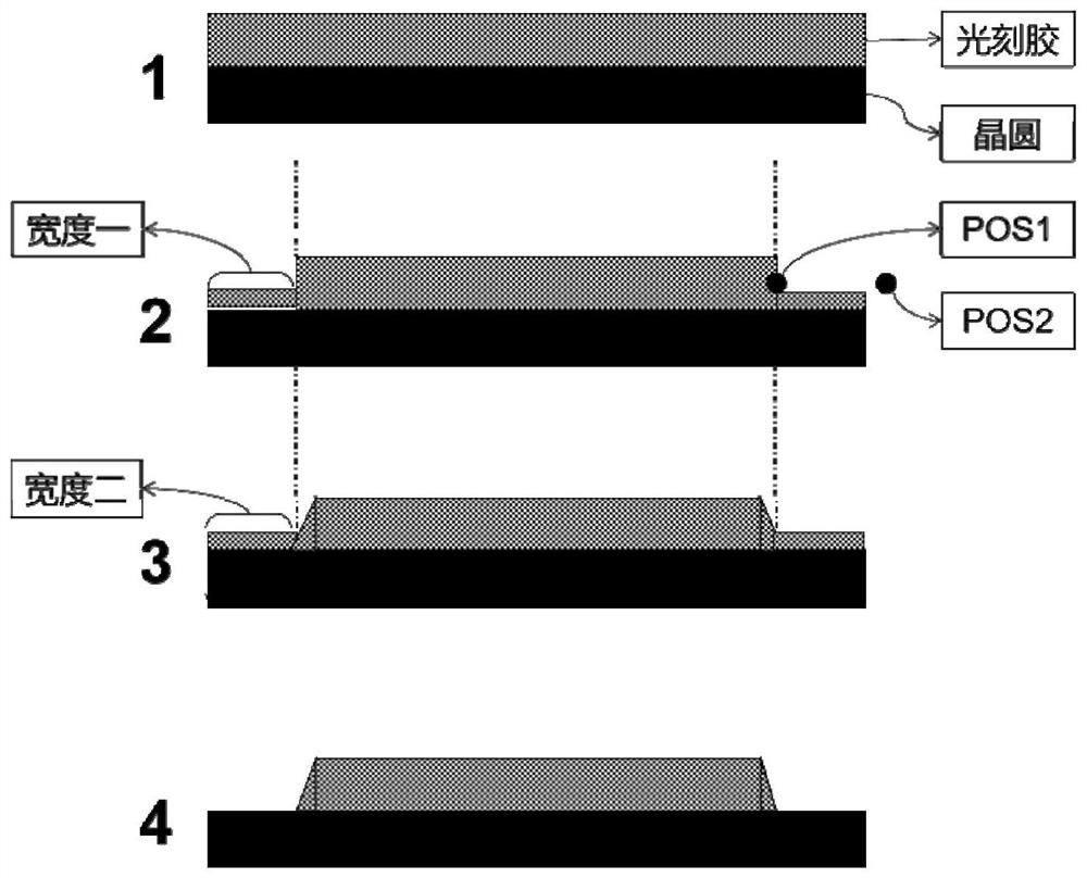
[0044] A certain photoresist PI (same as Comparative Example 1) was used, the coating thickness was 7.7 μm, the edge removal target was W1=W2=1±0.1 mm, the chemical removal solution was OK73, and the wafer was a silicon wafer with a diameter of 300 mm. Such as image 3 As shown, combining chemical removal with edge exposure, adjusting various parameters and trying a variety of time combinations, the best removal effect of this method is obtained. The chemical edge removal takes 11s, the edge exposure takes 42s, the total time is 148.5s, the required amount of chemical solution is 3.6ml, the edge removal effect is better, reaching the spec, and the slope width is about 0.02mm.

[0045] From the recorded data, it can be found that for this embodiment, the method of the present invention has the best effect. Considering the time length, the amount of chemicals used, and the removal effect comprehensively, the method achieves the purpose of the invention.

Embodiment 2

[0051] A certain positive photoresist (same as Comparative Example 3) was used, the coating thickness was 15 μm, the edge removal target was W1=W2=1.3±0.15 mm, the chemical removal solution was OK73, and the wafer was a silicon wafer with a diameter of 300 mm. Such as image 3 As shown, combining chemical removal with edge exposure, adjusting various parameters and trying a variety of time combinations, the best removal effect of this method is obtained. It takes 8s to remove the edge, 15s to expose the edge, and the total time is 101s. The amount of chemical solution required is 2.6ml. The edge removal effect is better, reaching the spec, and the slope width is about 0.02mm.

[0052] From the recorded data, it can be found that for this embodiment, the method of the present invention has the best effect. Considering the time length, the amount of chemicals used, and the removal effect comprehensively, the method achieves the purpose of the invention.

[0053] Through the abo...


PUM

PropertyMeasurementUnit
Thicknessaaaaaaaaaa
Thicknessaaaaaaaaaa
Thicknessaaaaaaaaaa

Abstract

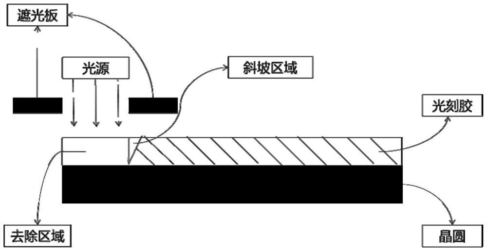
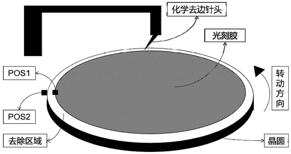
The invention discloses a method for removing a thick glue edge on a wafer, belonging to the technical field of semiconductor photoetching. According to the method, the thick glue (7-20 microns) edge on the wafer is removed. The method comprises the following steps that firstly, the thickness of a glue film in an edge area of the wafer is reduced in a chemical mode; and then thorough removal is carried out in an edge exposure mode. Compared with the prior art, the method of the invention has the advantages that time for removing photoresist on the thick glue edge is shortened; and by adjusting various technological parameters, on the premise of ensuring edge removal effect, productivity is improved, the consumption of chemical edge removal liquid and the edge exposure time are reduced, and the effects of reducing cost and increasing yield are achieved.

Description

technical field [0001] The invention relates to the technical field of semiconductor photolithography, in particular to a method for removing the edge of thick glue on a wafer. Background technique [0002] In semiconductor lithography process, as the critical dimensions of devices become smaller and smaller, the cleaning of the edge of the wafer becomes more important. The reasons include but are not limited to the following three points: 1. The photoresist is subjected to centrifugal force during the coating process. During the coating process, the glue will flow to the edge of the wafer. Due to its surface tension, a ring of glue droplets will be formed on the edge. If it is not removed, these glue droplets will peel off and form particles, causing pollution to the equipment and the wafer itself, and more serious pollution may occur Photolithography machine, resulting in poor exposure focus, increased overlay error, and increased defect rate; 2. Photoresist is easy to acc...

Claims


Application Information

Patent Timeline
IPC IPC(8): G03F7/16G03F7/40
CPCG03F7/168G03F7/40
Inventor 关丽孙洪君邢栗张晨阳张德强王延明朴勇男
Owner SHENYANG KINGSEMI CO LTD
Learn More