Four-dimensional invisible wave-absorbing structure and preparation method thereof
A wave structure and four-dimensional technology, applied in the field of four-dimensional stealth wave-absorbing structure and its preparation, can solve the problems of unrealized integration of honeycomb periodic wave-absorbing structure, increase of electromagnetic wave propagation path, easy falling off of impregnated coating, etc., and achieve simple and efficient processing procedures , Stable electromagnetic properties, low specific density
- Summary
- Abstract
- Description
- Claims
- Application Information
AI Technical Summary
Problems solved by technology
Method used
Image
Examples
Embodiment 1
[0049] This embodiment discloses a four-dimensional stealth absorbing structure, such as figure 1 As shown, a plurality of honeycomb periodic structure units 1 are included, and electromagnetic periodic structures 2 are arranged on the inner walls of at least some of the honeycomb periodic structure units.
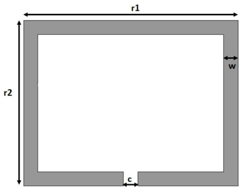
[0050] In this embodiment, the electromagnetic periodic structure may be in the form of a split resonant ring, an electric dipole, an H-shaped form, a figure-shaped form, or the like. like Figure 2a and 2b As shown, the split resonant ring can be a single rectangular split ring or a double rectangular split ring. Electric dipoles can be bow-tie, T-shaped, or round, etc.
[0051] When the split resonator ring is a single rectangular split ring, the opening of the single rectangular split ring faces downward relative to the incident direction of the electromagnetic wave, such as Figure 2a shown;
[0052] When the split resonant ring is a double rectangular split ring,...
Embodiment 2
[0060] This embodiment discloses a preparation method for realizing the four-dimensional stealth absorbing structure described in Embodiment 1, including:
[0061] Step 1. Use high-performance paper-based materials as the base material. In this embodiment, the paper base material may be aramid paper, PBO paper or multi-layer dielectric paper base material. Among them, the dielectric constant of the aramid paper is 2.7, and the magnetic permeability is 1, and the dielectric constant of the PBO paper is 1.44, and the magnetic permeability is 1. In this embodiment, when the base material is a multi-layer dielectric paper-based material, such as three layers, the uppermost layer and the lowermost layer use aramid paper or PBO paper, and the middle layer uses carbon fiber conductive paper, wherein the carbon fiber The weight percent content can be set to 1-20%. By adjusting the content of carbon fiber, the dielectric constant of the multilayer dielectric paper base material can be...
PUM
| Property | Measurement | Unit |
|---|---|---|
| length | aaaaa | aaaaa |
| length | aaaaa | aaaaa |
| width | aaaaa | aaaaa |
Abstract
Description
Claims
Application Information
 - R&D
- Intellectual Property
- Life Sciences
- Materials
- Tech Scout
- Unparalleled Data Quality
- Higher Quality Content
- 60% Fewer Hallucinations
Browse by: Latest US Patents, China's latest patents, Technical Efficacy Thesaurus, Application Domain, Technology Topic, Popular Technical Reports.
© 2025 PatSnap. All rights reserved.Legal|Privacy policy|Modern Slavery Act Transparency Statement|Sitemap|About US| Contact US: help@patsnap.com


