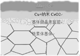
CeO2-doped Cu/Mn composite film/microcrystalline interface layer and metal matrix composite connector and preparation method thereof
A metal-based composite and interface layer technology, which is applied in coatings, final product manufacturing, sustainable manufacturing/processing, etc., can solve problems such as poor commercialization prospects and poor electrical conductivity, and achieve shortened reaction stability time and high electrical conductivity. , The effect of fine and uniform grain size
- Summary
- Abstract
- Description
- Claims
- Application Information
AI Technical Summary
Problems solved by technology
Method used
Image
Examples
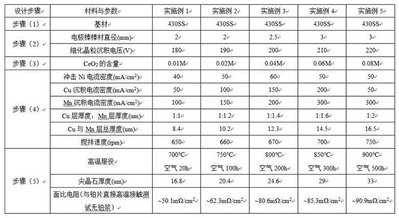
Embodiment 1
[0021] Step (1) The 430SS base material is polished with 400#~2000# water-grinding paper, then cleaned with distilled water and acetone, air-dried or blow-dried, and sealed for storage.
[0022] Step (2) Deposit a layer of flat 430SS fine grain transition layer on the surface of the substrate by high-temperature micro-arc alloying technology with an electrode rod with a diameter of 2mm, adjust the voltage to 180V, and prepare 430SS fine grain transition layer on the surface of the substrate. Grain layer, and then the prepared refined grain layer is repaired and flattened.
[0023] Step (3) First configure 400ml of electrolyte solution in a beaker for impact Ni plating, first pour 200ml of distilled water into the beaker, and then add 1M NiCl 2 , stirred until no precipitate was added, and then 128 mL of HCl was added and distilled water was gradually added to 400 mL. Configure 400ml electrolyte solution to electrodeposit Cu, first pour 300ml distilled water into the beaker, t...
Embodiment 2
[0027] Step (1) The 430SS base material is polished with 400#~2000# water-grinding paper, then cleaned with distilled water and acetone, air-dried or blow-dried, and sealed for storage.
[0028] Step (2) Deposit a layer of smooth 430SS fine grain transition layer on the surface of the substrate by high-temperature micro-arc alloying technology with an electrode rod with a diameter of 2mm, adjust the voltage to 190V, and prepare 430SS fine grain transition layer on the surface of the substrate. Grain layer, and the prepared refined grain layer is repaired and flattened.
[0029] Step (3) First configure 400ml of electrolyte solution in a beaker for impact Ni plating, first pour 200ml of distilled water into the beaker, and then add 1M NiCl 2 , stirred until no precipitate was added, and then 128 mL of HCl was added and distilled water was gradually added to 400 mL. Prepare 400ml of electrolytic deposition Cu electrolyte solution, first pour 300ml of distilled water into the be...
Embodiment 3
[0033] Step (1) The 430SS base material is polished with 400#~2000# water-grinding paper, then cleaned with distilled water and acetone, air-dried or blow-dried, and sealed for storage.
[0034] Step (2) Deposit a layer of flat 430SS fine grain transition layer on the surface of the substrate by high-temperature micro-arc alloying technology with an electrode rod with a diameter of 2.5mm, adjust the voltage to 200V, and prepare 430SS fine grain transition layer on the surface of the substrate. refine the grain layer, and repair and smooth the prepared grain refinement layer.
[0035] Step (3) First configure 400ml of electrolyte solution in a beaker for impact Ni plating, first pour 200ml of distilled water into the beaker, and then add 1M NiCl 2 , stirred until no precipitate was added, and then 128 mL of HCl was added and distilled water was gradually added to 400 mL. Prepare 400ml of electrolyte solution for electrodeposition Cu, first pour 300ml of distilled water into th...
PUM
| Property | Measurement | Unit |
|---|---|---|
| thickness | aaaaa | aaaaa |
| thickness | aaaaa | aaaaa |
Abstract
Description
Claims
Application Information
 - R&D Engineer
- R&D Manager
- IP Professional
- Industry Leading Data Capabilities
- Powerful AI technology
- Patent DNA Extraction
Browse by: Latest US Patents, China's latest patents, Technical Efficacy Thesaurus, Application Domain, Technology Topic, Popular Technical Reports.
© 2024 PatSnap. All rights reserved.Legal|Privacy policy|Modern Slavery Act Transparency Statement|Sitemap|About US| Contact US: help@patsnap.com


