High-power semiconductor optical amplifier

An optical amplifier and semiconductor technology, applied in semiconductor amplifier structures, semiconductor lasers, lasers, etc., can solve the problems of spot mode matching, difficult to achieve single mode, and reduce device gain, and achieve increased saturation output power, increase saturation output power and gain, the effect of improving small signal gain

Pending Publication Date: 2021-03-30
浙江长芯光电科技有限公司
View PDF0 Cites 1 Cited by
  • Summary
  • Abstract
  • Description
  • Claims
  • Application Information

AI Technical Summary

Problems solved by technology

Therefore, in the prior art, two types of waveguide structures based on slab-coupled epitaxial waveguide and tapered amplified structure are proposed. Based on the slab-coupled epitaxial structure, the N-waveguide layer is generally about 4-5um to increase mode broadening. This structure There are two disadvantages. One is that the thick N-waveguide layer makes the heat dissipation of the device poor; the other is that to broaden the optical field to the N-waveguide layer, it is necessary to sacrifice the logarithm of the quantum wells in the active layer and reduce the gain of the device.
Tapered semiconductor optical amplifiers generally obtain high saturated output power by increasing the width of the active region, but this structure will parasitic high-order modes, making it difficult to achieve single-mode, and its spot mode is still difficult to match the size of single-mode fiber

Method used


Image

  • High-power semiconductor optical amplifier
  • High-power semiconductor optical amplifier

Examples


Embodiment Construction

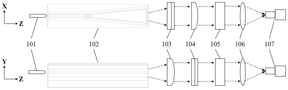
[0019] The technical scheme of the present invention will be further described below in conjunction with the accompanying drawings of the description:

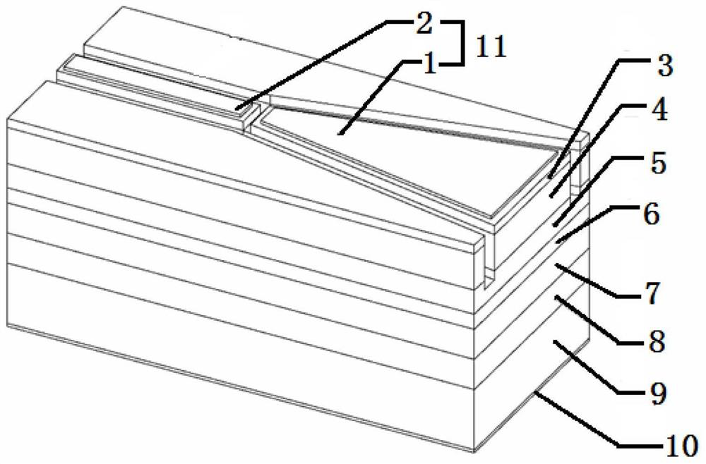
[0020] Such as figure 1 As shown, a high-power semiconductor optical amplifier includes an amplification region electrode 11, an electrode contact layer 3, an upper confinement layer 4, an upper waveguide layer 5, an active layer 6, a lower waveguide layer 7, and a lower confinement layer from top to bottom. 8. The substrate layer 9 and the N-surface electrode area 10. The electrode 11 of the amplification area is composed of the P-surface electrode 1 of the tapered amplification area and the P-surface electrode 2 of the ridge-shaped single-mode amplification area. The P-surface electrode 1 of the tapered amplification area The electrode 2 on the P surface and the ridge-shaped single-mode amplification region are electrically insulated from each other.

[0021] Such as figure 1 As shown, the difference between the refractive...


PUM

PropertyMeasurementUnit
widthaaaaaaaaaa
lengthaaaaaaaaaa
thicknessaaaaaaaaaa

Abstract

The invention discloses a high-power semiconductor optical amplifier, which is characterized by sequentially comprising an amplification region electrode, an electrode contact layer, an upper limitinglayer, an upper waveguide layer, an active layer, a lower waveguide layer, a lower limiting layer, a substrate layer and an N-surface electrode region from top to bottom. The amplification region electrode consists of a conical amplification region P-surface electrode and a ridge-shaped single-mode amplification region P-surface electrode; and the conical amplification region P-surface electrodeand the ridge-shaped single-mode amplification region P-surface electrode are electrically insulated from each other. According to the invention, the saturation output power and the small signal gainare improved, the problems of poor heat dissipation and low gain based on a flat plate coupling epitaxial structure are solved, the saturation output power can be improved to the watt level, and the small signal gain can break through 28dB.

Description

technical field [0001] The invention relates to a high-power semiconductor optical amplifier. Background technique [0002] Semiconductor optical amplifiers have been severely challenged by optical fiber amplifiers for quite a period of time, especially in optical fiber communications. The advantage of optical fiber amplifiers is that they can directly perform low-loss fusion splicing with transmission optical fibers, and have the advantages of small polarization correlation, low noise index, and high output power, which seriously squeezes the wavelength division multiplexing application of semiconductor optical amplifiers in the C+L band. . [0003] In recent years, with the rapid development of free space optical communication, laser radar and other fields, semiconductor optical amplifiers have low power consumption, small size, low cost, compatibility with COMS technology, simple electric pump structure, wide wavelength range, and radiation resistance. Strong and other ...

Claims


Application Information

Patent Timeline
Patent Type & Authority Applications(China)
IPC IPC(8): H01S5/02251H01S5/02253H01S5/042H01S5/34H01S5/50
CPCH01S5/34H01S5/50H01S5/04254
Inventor 杨明来
Owner 浙江长芯光电科技有限公司
Why Eureka
Try Eureka