SiC MOSFET (Metal Oxide Semiconductor Field Effect Transistor) device of integrated gate protection structure

A protection structure and integrated gate technology, applied in the field of semiconductors, can solve the problems of complex and fragile drive circuits, gate dielectric breakdown failure, reduced gate life and reliability, etc.

Pending Publication Date: 2021-01-15
安徽芯塔电子科技有限公司
View PDF0 Cites 3 Cited by
  • Summary
  • Abstract
  • Description
  • Claims
  • Application Information

AI Technical Summary

Problems solved by technology

However, in actual circuit applications, there are often some disturbances in current and voltage, such as sudden opening and closing of loads, circuit failures, external electromagnetic interference, etc., which may cause voltage fluctuations in the gate. If the gate voltage The fluctuation range exceeds the allowable range of the gate voltage, which will reduce the life and reliability of the gate, and even directly cause the breakdown of the gate dielectric
In order to avoid this phenomenon and protect the gate, a gate protection circuit is often set in the drive circuit in circuit applications, which not only increases the cost, but also makes the drive circuit complex and fragile

Method used


Image

  • SiC MOSFET (Metal Oxide Semiconductor Field Effect Transistor) device of integrated gate protection structure
  • SiC MOSFET (Metal Oxide Semiconductor Field Effect Transistor) device of integrated gate protection structure
  • SiC MOSFET (Metal Oxide Semiconductor Field Effect Transistor) device of integrated gate protection structure

Examples


Embodiment 1

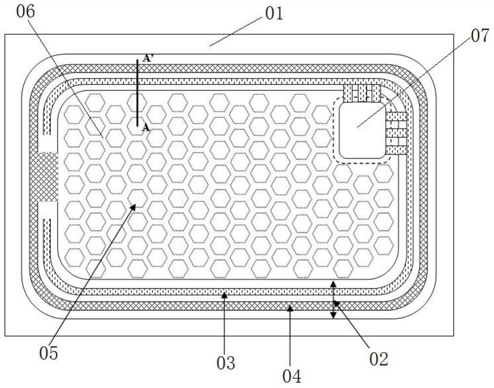
[0030] combine figure 1 , image 3 and Figure 5 As shown, this embodiment provides a SiC MOSFET device with an integrated gate protection structure. The SiC MOSFET device includes a scribe groove area and a terminal area 01, a p+ main ring 02, and a p+ main ring 02 in sequence from the edge to the center. The gate track 03 and the source track 04 on the grid, the active area composed of multiple primary cell structures 05 connected in parallel, and the source compact metal 06 and the gate compact metal 07 on the active area; the gate track 03 and the Two or more anti-series polysilicon pn diode structures are integrated between the source track 04 as the gate protection structure of the device.

[0031]A pair of anti-series polysilicon pn diodes D1 and D2 are connected in parallel between the gate and source. The breakdown voltage of D1 and D2 is designed according to the following design. When the gate forward voltage drop is greater than the maximum allowable forward volt...

Embodiment 2

[0042] combine figure 1 , Figure 4 and Figure 5 As shown, this embodiment provides a SiC MOSFET device with an integrated gate protection structure. The SiC MOSFET device includes a scribe groove area and a terminal area 01, a p+ main ring 02, and a p+ main ring 02 in sequence from the edge to the center. The gate raceway 03 and the source raceway 04, the active region composed of multiple primary cell structures 05 connected in parallel, and the source block metal 06 and gate block metal 07 on the active region; the p+ main ring 02 and The gate raceway 03 also exists in the middle region of the SiC MOSFET device to further reduce the unevenness of the gate voltage between the internal cells; two or more gate raceways 03 and the source block metal 06 are integrated The anti-series polysilicon pn diode structure is used as the gate protection structure of the device. At this time, a gate protection structure is integrated between the gate track 03 and the source block meta...


PUM

PropertyMeasurementUnit
thicknessaaaaaaaaaa
thicknessaaaaaaaaaa
thicknessaaaaaaaaaa

Abstract

The invention relates to the technical field of semiconductors and particularly relates to a SiC MOSFET device with an integrated gate protection structure. The device sequentially comprises a scribing groove region, a terminal region, a p + main ring, a gate runway and a source runway on the p + main ring, an active region formed by connecting a plurality of primitive cell structures in parallel,and pressing block metal of a source and a gate on the active region from the edge to the center, the device is characterized in that two or more polycrystalline silicon pn diode structures which arereversely connected in series are integrated between the gate runway and the source runway to serve as a gate protection structure of the device. According to the device, the gate protection device is integrated on the chip, when the gate voltage of the device exceeds the maximum allowable voltage, the gate protection device is broken down, so the gate source voltage is clamped at the maximum allowable voltage, and the MOS gate medium is protected from bearing high voltage.

Description

technical field [0001] The invention relates to the technical field of semiconductors, in particular to a SiC MOSFET device with an integrated gate protection structure. Background technique [0002] Compared with Si, the wide bandgap semiconductor material SiC has about 3 times the bandgap width, 10 times the critical breakdown electric field strength, and 3 times the thermal conductivity. Therefore, SiC devices have the advantages of higher withstand voltage, higher operating frequency and higher temperature resistance compared with Si devices. Both theory and practice have confirmed that SiC MOSFET has a switching frequency of more than 10 and better switching efficiency than Si-based IGBT, so SiC devices will have a very large application field and market. [0003] There are two kinds of atoms, Si and C, in the SiC material, so the thermal oxidation mechanism is much more complicated than that of the Si material, making SiC / SiO in the SiCMOS structure 2 The interface s...

Claims


Application Information

Patent Timeline
Patent Type & Authority Applications(China)
IPC IPC(8): H01L27/02H01L27/06
CPCH01L27/0255H01L27/0629
Inventor 倪炜江
Owner 安徽芯塔电子科技有限公司
Why Eureka
Try Eureka