Simulation method for multi-gate-finger gallium nitride device electric heating joint modeling

A technology of gallium nitride device and simulation method, which is applied in the fields of instruments, electrical digital data processing, special data processing applications, etc. The effect of improving output efficiency

Inactive Publication Date: 2021-01-05
SOUTH CHINA UNIV OF TECH +1
View PDF9 Cites 0 Cited by
  • Summary
  • Abstract
  • Description
  • Claims
  • Application Information

AI Technical Summary

Problems solved by technology

The multi-gate finger structure reduces the area and also brings serious heat dissipation problems. Due to the short distance between the multi-gate fingers, the heat-generating parts are concentrated. The closer the heat source is to the middle position, the harder it is to dissipate the heat. Up to hundreds of degrees Celsius, will seriously affect the performance of the device or even destroy the device or chip
The traditional single-gate model can only analyze the heat generation of a single device, and cannot predict the interaction between multiple gates and multiple heat sources

Method used


Image

  • Simulation method for multi-gate-finger gallium nitride device electric heating joint modeling
  • Simulation method for multi-gate-finger gallium nitride device electric heating joint modeling
  • Simulation method for multi-gate-finger gallium nitride device electric heating joint modeling

Examples


Embodiment Construction

[0023] A simulation method for electrothermal joint modeling of a multi-gate finger gallium nitride device according to the present invention, the following steps are performed in sequence:

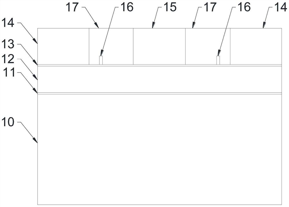
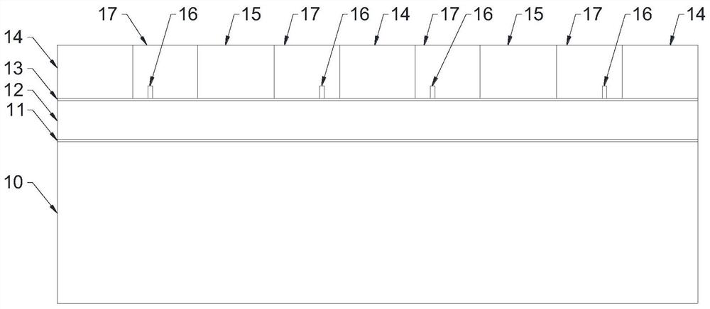
[0024] First, a two-dimensional model structure of a GaN device with multiple gate fingers is constructed. The so-called multi-gate finger refers to a device structure with 2N gate indices, where N is a natural number, that is, the minimum gate index is two.

[0025] The structure of the two-dimensional model with grid index two is as follows figure 1 As shown, a substrate 10 , an aluminum nitride layer 11 , a gallium nitride layer 12 , and an aluminum gallium nitride layer 13 are stacked from bottom to top. A source 14 is arranged at both ends of the upper surface of the aluminum gallium nitride layer 13 , and a drain 15 is arranged in the middle. A gate 16 is respectively arranged between the two source electrodes 14 and the drain electrodes 15 , and the gate electrodes 16 are respect...


PUM


Abstract

The invention discloses a simulation method for multi-gate-finger gallium nitride device electro-thermal joint modeling, and belongs to a new generation of information technology. The scheme is provided for solving the problem that in the prior art, the mutual influence between multiple grids and multiple heat sources cannot be predicted. According to the invention, electro-thermal joint simulation of a device is realized by means of sequential two-dimensional model structure setting, doping setting, superposition of a physical field and a physical effect, boundary condition setting, mesh generation and the like; and the method has the advantages that the mutual influence among multiple heat sources after the self-heating effect of the device occurs can be more accurately predicted on theelectrical level of the device, the method is used for thermal management and thermal optimization occasions of the device on a chip and a circuit, and the output efficiency of the circuit can be improved.

Description

technical field [0001] The invention relates to an electronic device simulation method, in particular to a simulation method for electrothermal joint modeling of a multi-gate finger gallium nitride device. Background technique [0002] As a third-generation semiconductor, gallium nitride has been gradually recognized, understood and applied. Gallium nitride materials are made into high electron mobility devices through MOCVD and other processes. The principle is similar to that of NMOS devices. The difference is that the conductive channel of the former is induced by strain between the aluminum gallium nitride layer and the gallium nitride layer. The electron channel formed by the two-dimensional electron gas layer, so GaN high electron mobility devices are mostly depletion type without special processing. [0003] Whether in power management circuits or radio frequency circuits, the excellent performance of gallium nitride devices and chips makes them more widely used in h...

Claims


Application Information

Patent Timeline
Patent Type & Authority Applications(China)
IPC IPC(8): G06F30/398G06F119/08
CPCG06F30/398G06F2119/08
Inventor 李斌陈欣煌吴朝晖
Owner SOUTH CHINA UNIV OF TECH
Why Eureka
Try Eureka