A kind of deep ultraviolet light emitting diode based on electronic buffer and its manufacturing method

A technology of light-emitting diodes and electronic buffering, applied in circuits, electrical components, semiconductor devices, etc., can solve the problems of limited radiation recombination in the active area, hinder injection into the active area, and reduce the height of the valence band, so as to improve luminous efficiency and improve Radiative recombination rate, effect of slowing thermal transition speed

Active Publication Date: 2021-12-10
GUANGDONG INST OF SEMICON IND TECH
View PDF0 Cites 0 Cited by
  • Summary
  • Abstract
  • Description
  • Claims
  • Application Information

AI Technical Summary

Problems solved by technology

However, the AlGaN electron blocking layer with high Al composition will also reduce the height of the valence band, and will generate a large potential barrier for holes, which seriously hinders the injection of holes from the p-type semiconductor layer into the active region, so that there is Radiative recombination in the source region is limited

Method used


Image

  • A kind of deep ultraviolet light emitting diode based on electronic buffer and its manufacturing method
  • A kind of deep ultraviolet light emitting diode based on electronic buffer and its manufacturing method

Examples


no. 1 example

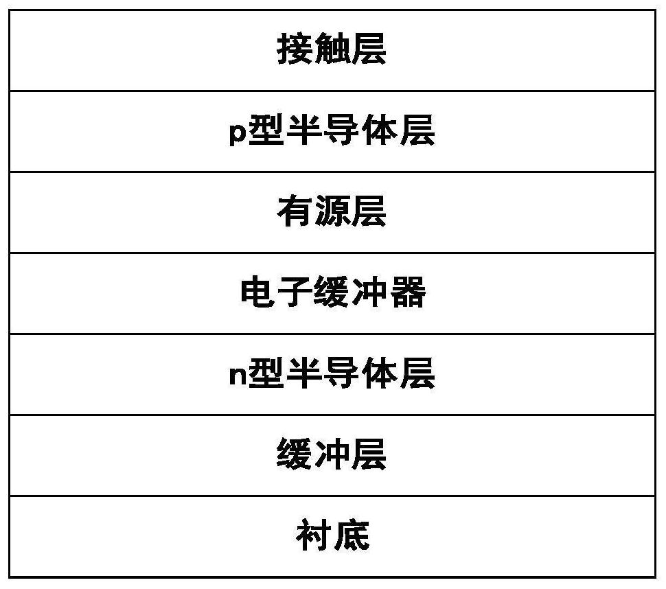
[0025] see figure 1 , an embodiment of the present invention is a deep ultraviolet light-emitting diode based on an electronic buffer. The deep ultraviolet light-emitting diode includes a substrate, a buffer layer that is epitaxially grown on the substrate, an n-type semiconductor layer, an electronic buffer, and an organic light-emitting diode. source layer, p-type semiconductor layer and contact layer, wherein the electron buffer is non-doped B x Al 1-x N-layer and n-type Al y Ga 1-y A multi-period composite structure in which N layers are alternately grown, and the last grown non-doped B in the multi-period composite structure x Al 1-x The N layer is in contact with the first barrier layer in the active layer.

[0026] In an embodiment of the present invention, the value range of x is: 0.01≤x≤0.3, and the value range of y is: 0.01≤y≤1.

[0027] In an embodiment of the present invention, each B in the electronic buffer x Al 1-x N layer and the B x Al 1-x Al on the ...

no. 2 example

[0034] see figure 2 , an embodiment of the present invention provides a method for manufacturing a deep ultraviolet light-emitting diode based on an electronic buffer. The method includes: providing a substrate; growing a buffer layer and an n-type semiconductor layer sequentially on the substrate using MOCVD equipment. Layer, electron buffer, active layer, p-type semiconductor layer and contact layer; Wherein, described electron buffer is B x Al 1-x N-layer and n-type Al y Ga 1-y A multi-period composite structure in which N layers are alternately grown, and the last grown non-doped B in the multi-period composite structure x Al 1-x The N layer is in contact with the first barrier layer in the active layer.

[0035] In a certain embodiment of the present invention, the manufacturing method is specifically:

[0036] S101. Provide a substrate;

[0037] S102, sequentially depositing a buffer layer and an n-type semiconductor on the substrate;

[0038] S103, depositing n...


PUM

PropertyMeasurementUnit
thicknessaaaaaaaaaa
thicknessaaaaaaaaaa

Abstract

The invention discloses a deep ultraviolet light-emitting diode based on an electronic buffer and a manufacturing method thereof. The deep ultraviolet light-emitting diode comprises: a substrate, a buffer layer epitaxially grown on the substrate, an n-type semiconductor layer, and an electronic buffer , active layer, p-type semiconductor layer and contact layer, wherein, the electron buffer is non-doped B x Al 1‑x N-layer and n-type Al y Ga 1‑y A multi-period composite structure in which N layers are alternately grown, and the last grown non-doped B in the multi-period composite structure x Al 1‑x The N layer is in contact with the first barrier layer in the active layer. The invention can significantly improve the hole injection in the active area of ​​the diode, effectively alleviate the electron leakage, increase the radiation recombination rate in the active area, and thereby improve the luminous efficiency of the ultraviolet LED.

Description

technical field [0001] The invention relates to the technical field of semiconductor devices, in particular to a deep ultraviolet light-emitting diode based on an electronic buffer and a manufacturing method thereof. Background technique [0002] Ultraviolet light-emitting diodes (LEDs) have the advantages of environmental protection and non-toxicity, low power consumption, small size and long life, and meet the requirements of environmental protection and energy saving in the new era. It has important application value in the fields of ultraviolet curing, sterilization and disinfection, air and water purification, biomedicine, high-density storage, safe and secure communication, etc. [0003] A UV LED generally includes an epitaxial wafer and electrodes prepared on the epitaxial wafer. The AlGaN-based ultraviolet LED epitaxial wafer generally includes: a substrate and a buffer layer, an n-type semiconductor layer, an active layer, an electron blocking layer, a p-type semic...

Claims


Application Information

Patent Timeline
Patent Type & Authority Patents(China)
IPC IPC(8): H01L33/14H01L33/32H01L33/00
CPCH01L33/14H01L33/32H01L33/0075
Inventor 贺龙飞吴华龙张康何晨光刘云洲赵维陈志涛
Owner GUANGDONG INST OF SEMICON IND TECH
Why Eureka
Try Eureka