


Quick Research
Generate reliable direction feasibility study reports for your R&D in just a few steps.

Technical Q&A
Discover and master advanced knowledge NOW. Basics, ideas, possibilities, all at once.

Find Solutions
As an expert in R&D theories, this can generate solutions to your technical problems instantly.

Evaluate Feasibility
Analyze your overall solution with one click, know your potential R&D risks in advance.

Monitor Landscape
Get weekly tech updates, stay abreast of the latest tech innovations and key insights.
Preparation method of light modulation terahertz absorption device with all-carbon structure
A carbon structure, terahertz technology, applied in optical components, instruments, optics, etc., can solve the problems of difficult processing of single-layer graphene, inability to carry out optical signals, low terahertz reflection intensity, etc., to avoid low sublimation growth density, The effect of enhancing the terahertz signal and increasing the specific surface area
- Summary
- Abstract
- Description
- Claims
- Application Information
AI Technical Summary
Problems solved by technology
Method used
Image

Examples
Embodiment 1
[0040] (1) Assemble a graphene oxide solution (0.5ug / mL) on an anodized aluminum substrate by spin coating to form a graphene oxide film with a thickness of 40 atomic layers, and chemically reduce the graphene oxide film. The reduction condition is HI as the reducing agent, Treat at 60°C for 4h.
[0041] (2) FeCl 3 (100°C) is uniformly vapor-deposited on the surface of the reduced nano-film, cooled, solidified and shrunk to obtain an exfoliated graphene nano-film.
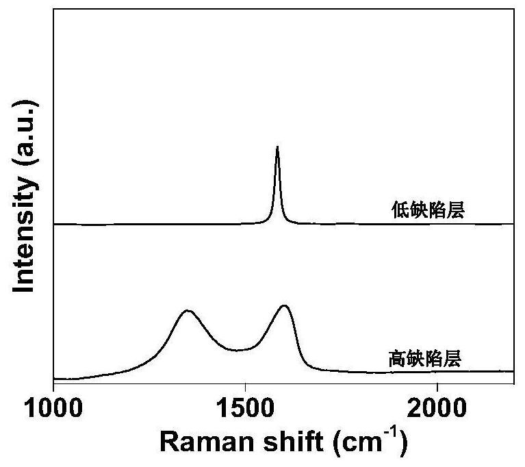
[0042] (3) With a heating rate of 10°C / min, the graphene oxide film was heated up to 1200°C by electric heating, and kept for 4h to obtain a graphene film layer with high defects and high terahertz transmission, with a defect content of 30%; the graphite oxide The temperature of the olefin film was raised to 2300 °C and kept for 2 h to reduce the defects of the graphene oxide film to 0.2%.
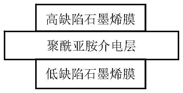
[0043] (4) The obtained high-defect graphene film and low-defect graphene film are attached to the front and back of the po...
Embodiment 2
[0045] (1) Assemble a graphene oxide solution (0.5ug / mL) on a glass fiber substrate to form a 60-atom-layer-thick graphene film by suction filtration, and then chemically reduce the nanofilm. The reduction condition is HI as the reducing agent, and 90 ° C for 2 hours .
[0046] (2) AlCl 3 (183°C) is uniformly vapor-deposited on the surface of the nano-film, cooled, solidified and shrunk to obtain an exfoliated graphene nano-film.
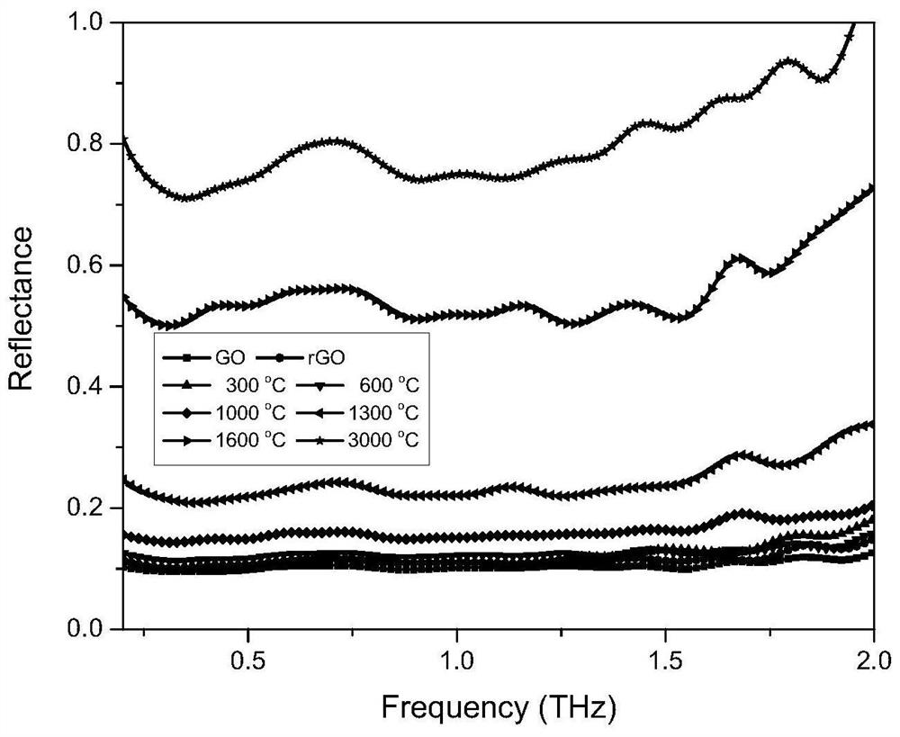
[0047] (3) With a heating rate below 20° C. / min, the graphene oxide film is heated by infrared radiation to 1300° C. and kept for 4 hours to obtain a graphene film layer with high defects and high terahertz transmission, and the defect content is 50% ( figure 1 , its SEM image is shown in Image 6 Shown); graphene oxide film is heated up to 2000 ℃, and keeps 4h, to reduce the defect of graphene oxide film to below 0.3% ( figure 1 ). As the temperature increases, the graphene structure is gradually repaired, and the terahertz reflection of the gr...
Embodiment 3
[0050] (1) Assemble graphene oxide (0.5ug / mL) on the mixed cellulose ester substrate by suction filtration to form a graphene film with a thickness of 180 atomic layers, and then chemically reduce the nanofilm.
[0051] (2) AlCl 3 (183°C) is evenly evaporated on the surface of the nanometer film, cooled and solidified to etch the substrate (mixed cellulose ester as the substrate), and the exfoliated graphene nanofilm is obtained.
[0052] (3) With a heating rate of 30°C / min, the graphene oxide film was heated to 1400°C by microwave heating, and kept for 2h to obtain a graphene film layer with high defects and high terahertz transmission, with a defect content of 20%; the graphite oxide The temperature of the olefin film was raised to 3000 °C and kept for 1 h to reduce the defects of the graphene oxide film to 0.3%.
[0053] (4) Attach the obtained high-defect graphene film and low-defect graphene film to the front and back of the polyimide film to form a flexible terahertz ab...
PUM
 Abstract
Description
Claims
Application Information
 - R&D Engineer
- R&D Manager
- IP Professional
- Industry Leading Data Capabilities
- Powerful AI technology
- Patent DNA Extraction
Browse by: Latest US Patents, China's latest patents, Technical Efficacy Thesaurus, Application Domain, Technology Topic, Popular Technical Reports.
© 2024 PatSnap. All rights reserved.Legal|Privacy policy|Modern Slavery Act Transparency Statement|Sitemap|About US| Contact US: help@patsnap.com