Large-format array femtosecond laser micro-fluidic chip direct printing method and equipment thereof

A microfluidic chip and femtosecond laser technology, which is applied in laser welding equipment, welding equipment, metal processing equipment, etc., can solve the problems of low technical efficiency and low intelligence in the preparation of microfluidic chips, and achieve the benefits of mass production. The effect of high preparation and processing stability and high degree of intelligence

Active Publication Date: 2021-01-01
CHONGQING INST OF EAST CHINA NORMAL UNIV +1
View PDF5 Cites 0 Cited by
  • Summary
  • Abstract
  • Description
  • Claims
  • Application Information

AI Technical Summary

Problems solved by technology

This method usually uses a single beam of light for scanning processing of microchannels or micro-functional parts. There are also related studies that use multiple beams of light for parallel processing of micro-functional parts. The method of parallel processing can improve the processing efficiency to a certain extent, but compared with Efficient and intelligent preparation technology for integrated circuit chips such as computers and mobile phones. At present, the efficiency and intelligence of microfluidic chip preparation technology are relatively low, and continuous technological innovation and development are still needed.

Method used


Image

  • Large-format array femtosecond laser micro-fluidic chip direct printing method and equipment thereof
  • Large-format array femtosecond laser micro-fluidic chip direct printing method and equipment thereof
  • Large-format array femtosecond laser micro-fluidic chip direct printing method and equipment thereof

Examples


Embodiment Construction

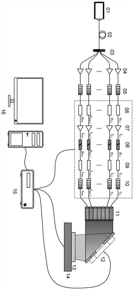
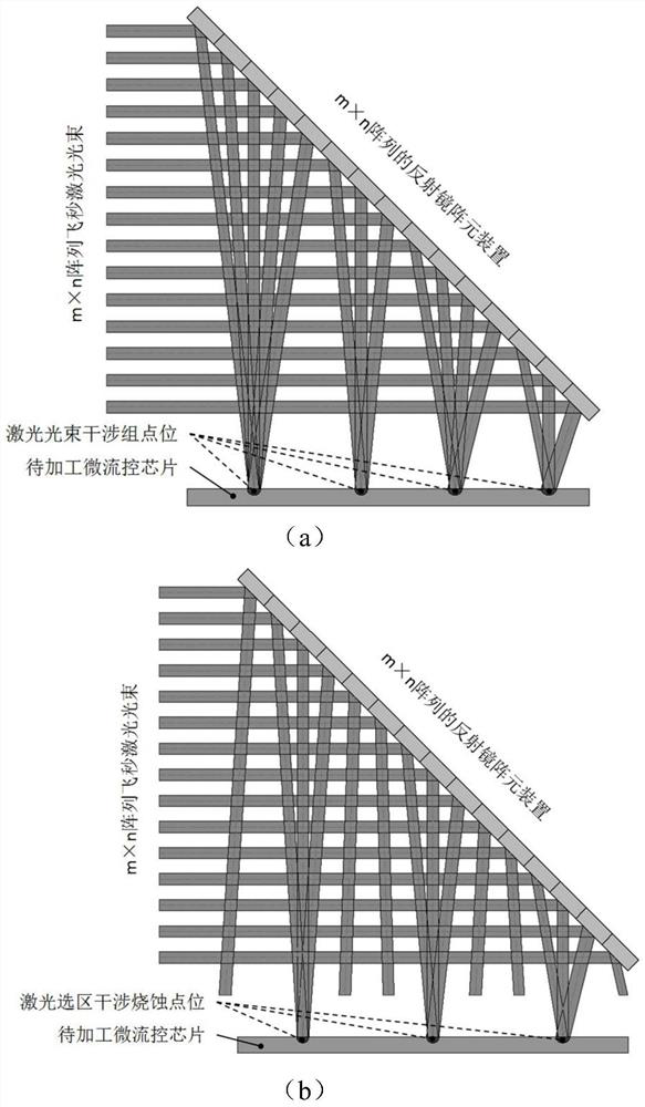
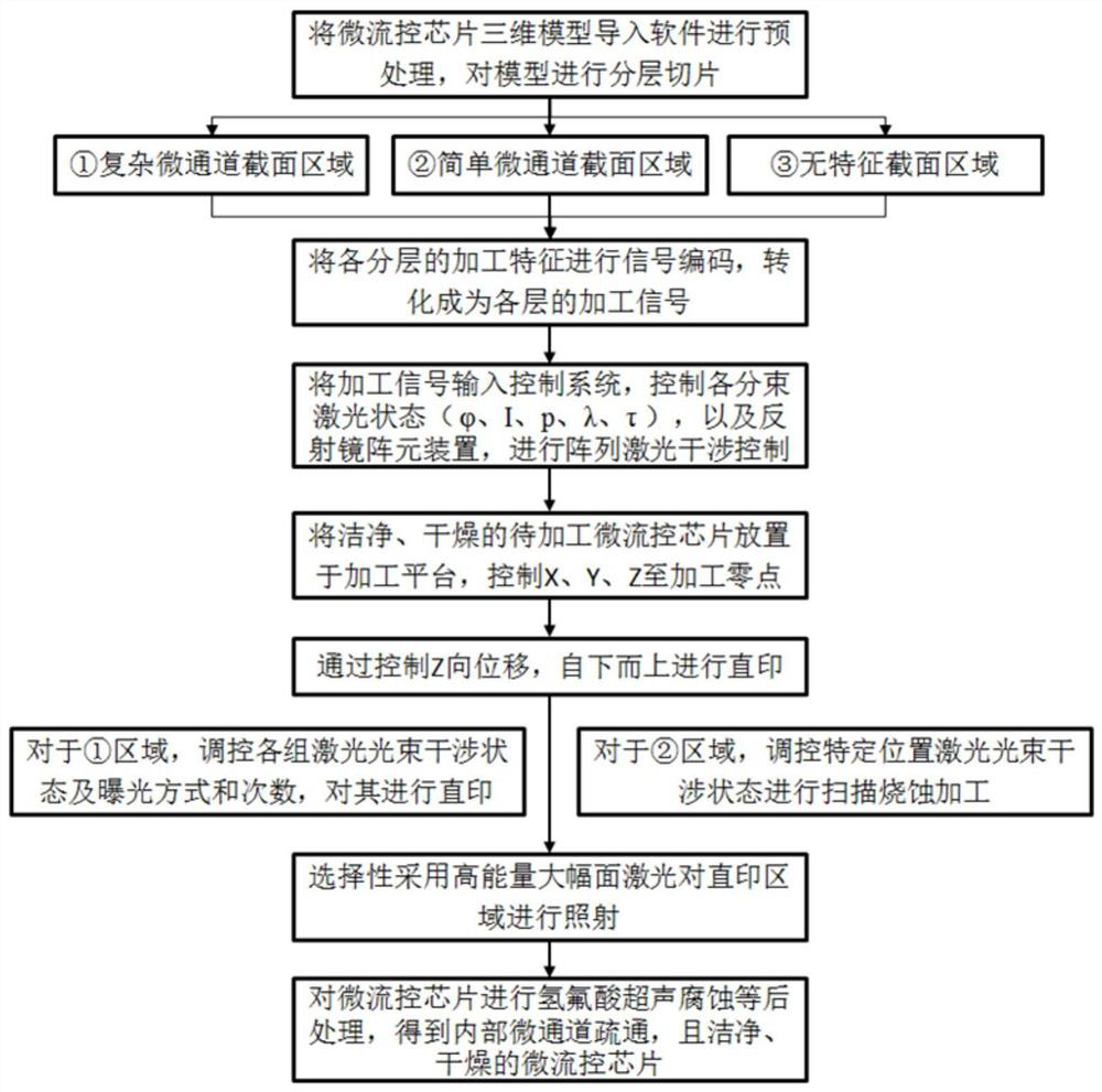
[0082] The following examples will further illustrate the present invention in conjunction with the accompanying drawings. This example is based on the method of femtosecond laser interference to realize the preparation technology of large-format array femtosecond laser direct printing microfluidic chips, but this example cannot be used to limit the present invention , all the similar methods of the present invention and similar changes thereof should be included in the protection scope of the present invention.

[0083] figure 1 The computer system (16) implements the phase modulator (06), the light intensity modulator (07), the polarization controller (08), the frequency multiplier (09), and the pulse compressor (10) through the integrated controller (15). control the phase φ, light intensity I, polarization p, center wavelength λ, and pulse width τ of each split laser beam, and realize the signal control of each mirror unit in the mirror array element device (12), and the t...


PUM


Abstract

The invention discloses large-format array femtosecond laser micro-fluidic chip direct printing equipment and method. Large-format laser interference is achieved through large-format array femtosecondlasers with adjustable laser beam states regulated and output, the large-format array femtosecond laser interference states, interference combinations and exposure modes are regulated and controlled,patterns to be machined of a micro-fluidic chip are output through multiple times of exposure superposition, and direct printing machining of the micro-fluidic chip is achieved. According to the invention, rapid processing of the micro-fluidic chip can be realized, the processing efficiency of the micro-fluidic chip is improved, the processing period of the micro-fluidic chip is shortened, and the micro-fluidic chip processing method has remarkable advantages in the aspect of processing the micro-fluidic chip with a complex three-dimensional structure and has a wide application prospect.

Description

technical field [0001] The invention belongs to the technical field of microfluidic chip processing, and in particular relates to a large-format array femtosecond laser microfluidic chip direct printing technology and equipment. Background technique [0002] Microfluidic chip technology conforms to the development trend of miniaturization, integration and intelligence, and integrates the experiments and analysis processes that need to be carried out in traditional laboratories on centimeter-sized chips, so as to realize systems in the fields of biology, chemistry, and medicine. Analyze the detection process. Integrated analysis and detection process and reagent micro-flow requirements The micro-channel structure of the micro-fluidic chip prepared by processing has the characteristics of micro-size, high-precision, complex structure, and true three-dimensional, so strict requirements are put forward for the processing technology of the micro-fluidic chip . Traditional micro...

Claims


Application Information

Patent Timeline
Patent Type & Authority Applications(China)
IPC IPC(8): B01L3/00B81C1/00
CPCB01L3/502707B81C1/00119B81C1/00547B23K26/0676B23K26/0624B23K26/36B23K26/032B23K26/0643G06F30/3308B81C1/00539
Inventor 曾和平杨川胡梦云袁帅
Owner CHONGQING INST OF EAST CHINA NORMAL UNIV
Why Eureka
Try Eureka