Preparation method of novel InGaN-based photo-anode
A photoanode, a new type of technology, applied in the field of semiconductor heterojunction preparation, can solve the problems of high stress in InGaN layer, limited photolysis water efficiency, strong polarization effect, etc., achieve high crystal quality, easy process conditions, and small polarization effect of effect
- Summary
- Abstract
- Description
- Claims
- Application Information
AI Technical Summary
Problems solved by technology
Method used
Image
Examples
Embodiment 1
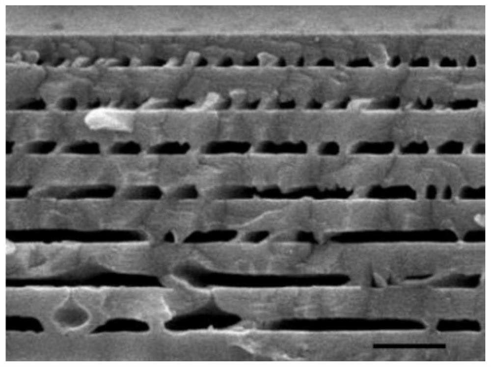
[0035] On the epitaxial substrate, a low-temperature GaN buffer layer and a GaN multilayer structure were grown successively, the growth temperature was 1070°C, the thickness of the low-doped GaN layer and the high-doped GaN layer were both 52nm, and the doping concentration of the low-doped GaN layer was 4.0× 10 15 , the doping concentration of the highly doped GaN layer is 2.5×10 19 , and the number of cycles is 7.
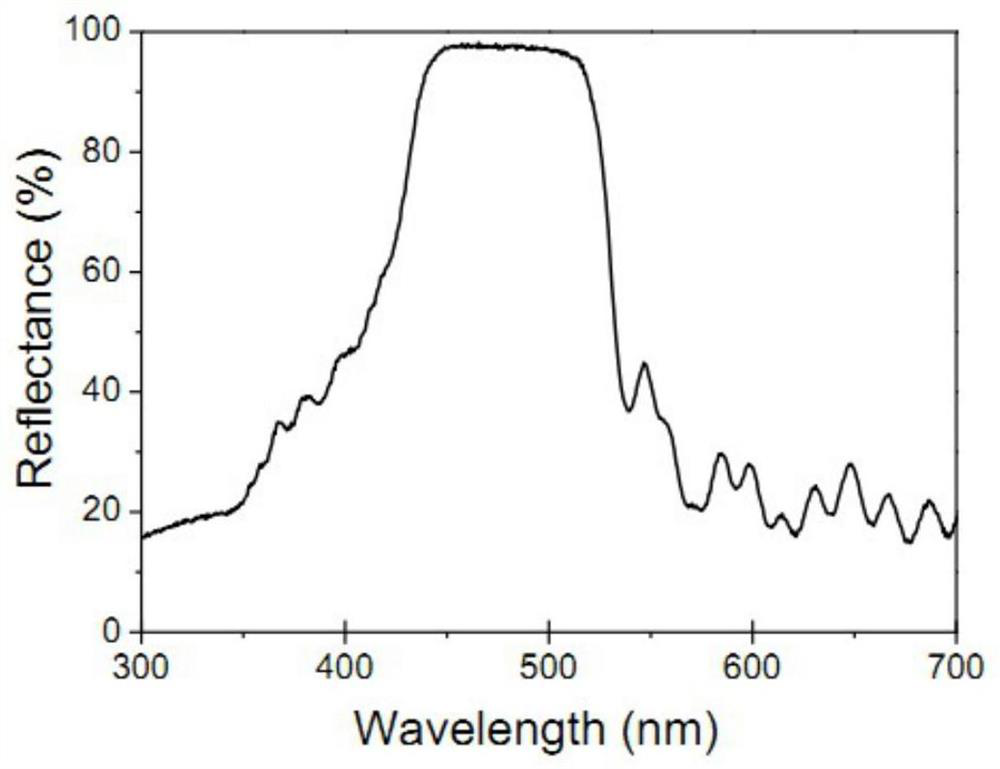
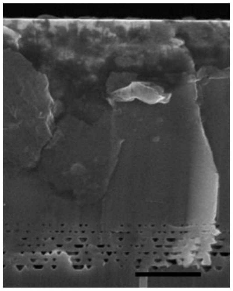
[0036] In a 0.1mol / L nitric acid solution, turn on the photoelectrochemical etching equipment, turn on the ultraviolet lamp, and set the etching voltage to 16V; use platinum wire as the cathode, and GaN multilayer structure as the anode, etch at a constant voltage for 40 Minutes; after the etching is finished, turn off the photoelectrochemical etching equipment; rinse the anode sample with deionized water, and dry it with nitrogen to obtain a mesoporous GaN mirror;
[0037] Using a mesoporous GaN mirror as a substrate, place the substrate in an MOCVD growth ch...
Embodiment 2
[0039] The low-temperature GaN buffer layer and the GaN multilayer structure were grown successively on the epitaxial substrate, the growth temperature was 1070°C, and the doping concentration of the low-doped GaN layer was 5.0×10 17 cm -3 , the thickness is 55nm, and the doping concentration of the highly doped GaN layer is 3.0×10 19 cm -3 , with a thickness of 52nm, a GaN multilayer structure is prepared;
[0040] In a 0.2mol / L nitric acid solution, turn on the photoelectrochemical etching equipment, turn on the white light, and set the etching voltage to 10V; use platinum wire as the cathode and GaN multilayer structure as the anode, etch at a constant voltage for 80 Minutes; after the etching is finished, turn off the photoelectrochemical etching equipment; rinse the anode sample with deionized water, and dry it with nitrogen to obtain a mesoporous GaN mirror;
[0041] Using a mesoporous GaN mirror as a substrate, place the substrate in an MOCVD growth chamber and grow ...
Embodiment 3
[0043] A low-temperature GaN buffer layer and a GaN multilayer structure were grown successively on the epitaxial substrate at a growth temperature of 1070°C, and the doping concentration and thickness of lightly doped GaN were 5.0×10 15 cm -3 and 50nm, heavily doped GaN doping concentration and thickness are 1×10 19 cm -3 and 65nm, a GaN multilayer structure was prepared. In a 0.3mol / L nitric acid solution, the photoelectrochemical etching equipment was turned on, and the etching voltage was set to 15V; the platinum wire was used as the cathode, and the GaN multilayer structure was used as the anode. , constant voltage etching for 20 minutes; after the etching, turn off the photoelectrochemical etching equipment; rinse the anode sample with deionized water, and dry it with nitrogen to obtain a mesoporous GaN mirror;
[0044] Using a mesoporous GaN mirror as a substrate, place the substrate in an MOCVD growth chamber and grow GaN at 1050 °C with a doping concentration of 8×1...
PUM
 Abstract
Description
Claims
Application Information
 - R&D
- Intellectual Property
- Life Sciences
- Materials
- Tech Scout
- Unparalleled Data Quality
- Higher Quality Content
- 60% Fewer Hallucinations
Browse by: Latest US Patents, China's latest patents, Technical Efficacy Thesaurus, Application Domain, Technology Topic, Popular Technical Reports.
© 2025 PatSnap. All rights reserved.Legal|Privacy policy|Modern Slavery Act Transparency Statement|Sitemap|About US| Contact US: help@patsnap.com


