Semiconductor light-emitting device and method for manufacturing the same

Active Publication Date: 2005-08-30
LEXINGTON LUMINANCE
View PDF5 Cites 52 Cited by
  • Summary
  • Abstract
  • Description
  • Claims
  • Application Information

AI Technical Summary

Benefits of technology

[0008]The aforementioned deficiencies are addressed, and an advance is made in the art, by using the substrate member comprising a textured surface district described in the present invention. The controlled layer deposition over the textured surface district proceeds such that the inclined layer growth in the trench region diminishes in the early stage of the process. Since the threading dislocations propagate along the growth direction, they are guided towards designated location and confined therein. The free propagation of the dislocation defects is thus restricted and the defect density in the active layer is significantly reduced. The textured district in the present invention comprises a plurality of smooth trenches without a prescribed angle of inclination. This allows for the nucleation of smooth semiconductor layers over the energetically favorable sites.
[0009]In the present invention, the substrate is patterned using conventional lithographic methods, followed by thermal anneal to smooth out sharp corners and etching defects. After thermal etching and solid-state diffusion, the stripe or mesa features become naturally rounded and free of surface irregularities. The textured surface district thus obtained is essential for the growth of smooth layers without the occurrence of chaotic micro-faceting.
[0010]The defect density is further reduced by using the mask to block the defect propagation. In this case, the mask district is spaced by a plurality of smooth trenches and the layer is allowed to dispose around the ledge of the mask. As a result, the free propagation of threading dislocations is further restricted by the mask district. The semiconductor member in the present invention is suitable for the low-cost, large area fabrication of misfit device structures.
[0011]Furthermore, the layer deposition around the mask district is altered by varying the aspect ratio of the mask. Due to the excessive supply of adatoms migrating from the mask surface, the thickness and alloy composition of the layer is modulated. As a result, the individual emitter disposed over the present mask district emits at a different wavelength of the spectrum. The chirped mask design in the present invention is useful to digitally synthesize the desirable color output of the light-emitting device by tailoring the light emission from its component emitters.

Problems solved by technology

As a result, the free propagation of threading dislocations is further restricted by the mask district.

Method used


Image

  • Semiconductor light-emitting device and method for manufacturing the same
  • Semiconductor light-emitting device and method for manufacturing the same
  • Semiconductor light-emitting device and method for manufacturing the same

Examples


Embodiment Construction

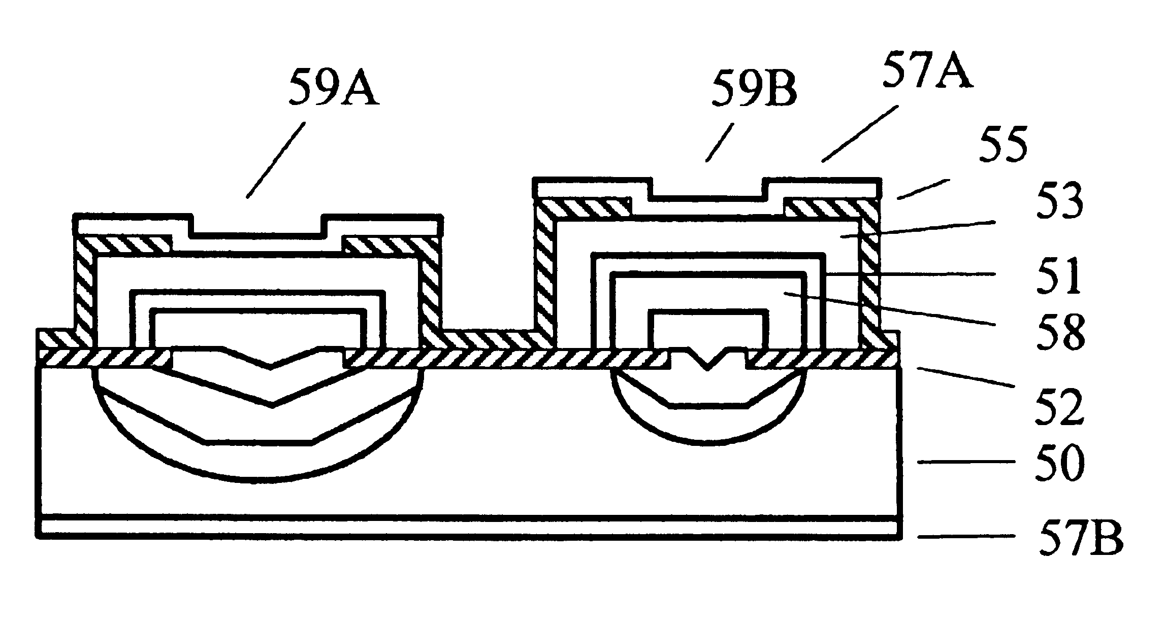
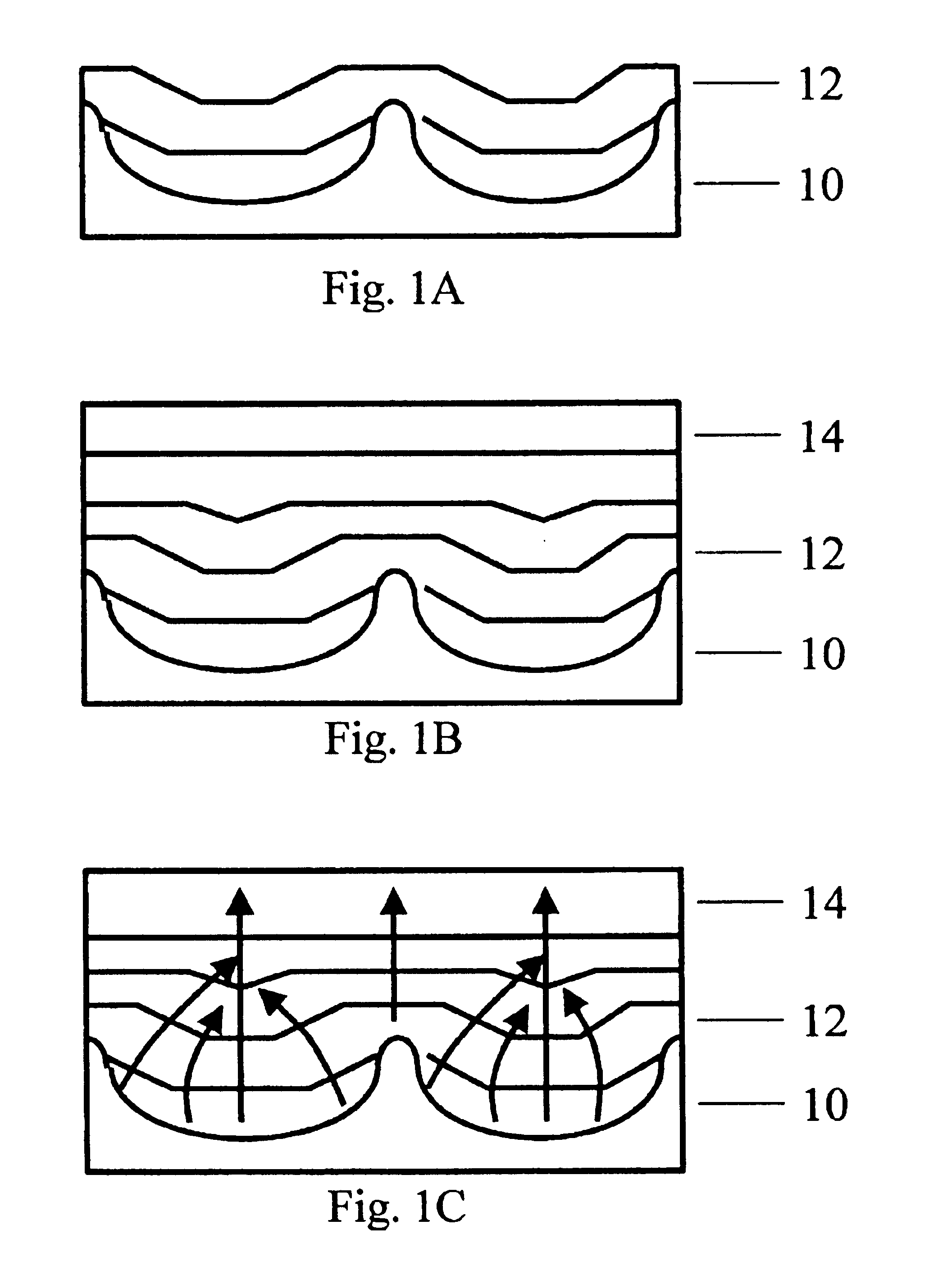
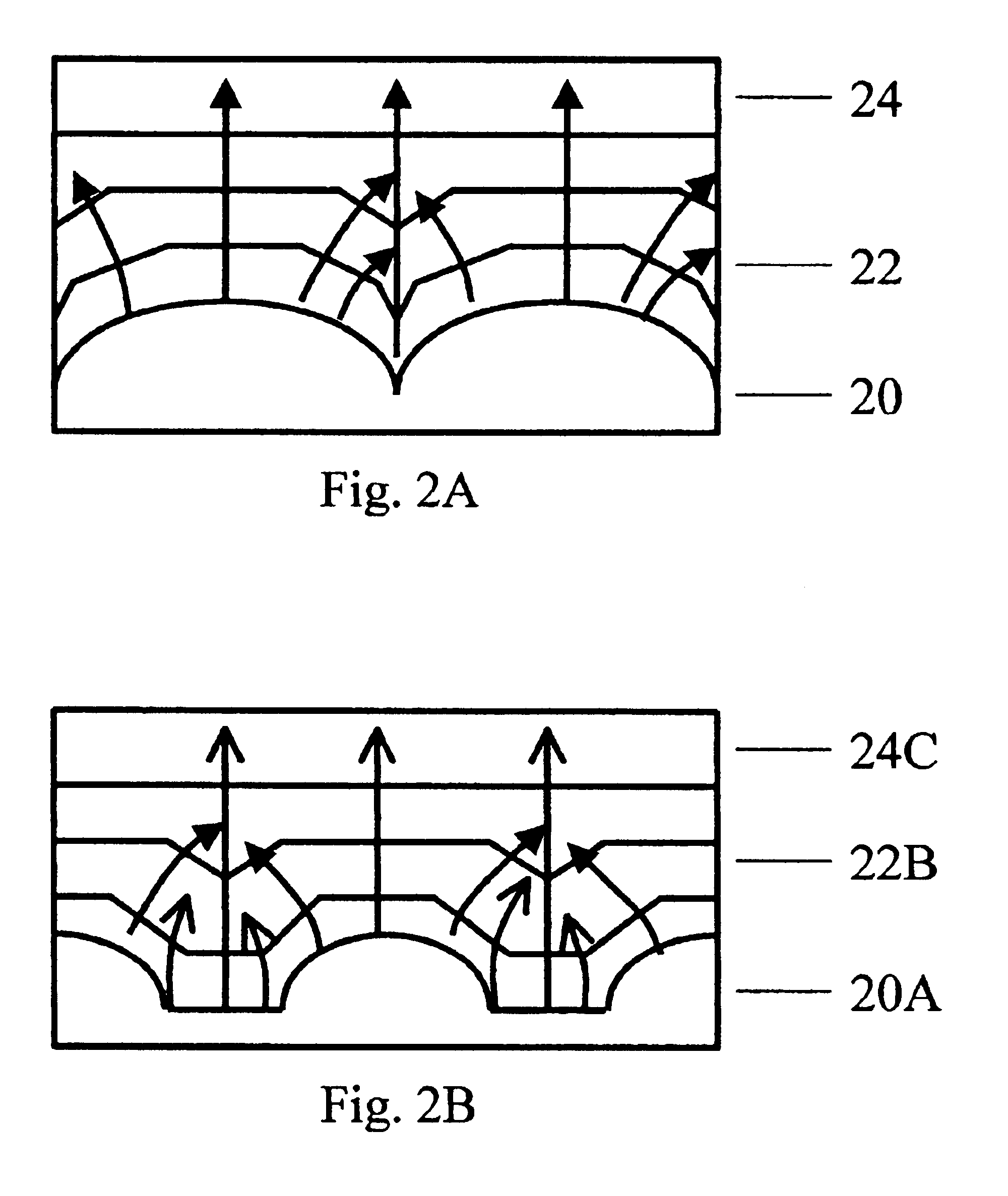
[0020]The semiconductor device in the present invention is fabricated on a substrate having a textured district defined on the substrate surface. The textured surface district comprises a plurality of etched features such as trenches and mesa having a smooth rotation of micro-facets. Accordingly, the direction of inclined layer growth is not uniquely prescribed by mesa etching. Instead, a spectrum of micro-facets is exposed to allow preferential layer nucleation over facets with energetically favorable sites. The epilayer deposition is solely determined by the growth chemistry and is less prone to the etching defects. As the inclined growth proceeds, the extended defects such as misfit dislocation are guided to designated locations and the overall defect density in the misfit system is reduced.

[0021]In accordance with an illustrative embodiment of the present invention, mesa or stripe features are first defined over the surface of the substrate using conventional photolithography et...


PUM


Abstract

Semiconductor light emitting device and methods for its manufacture comprises a plurality of textured district defined on the surface of the substrate. The initial inclined layer deposition serves to guide the extended defects to designated gettering centers in the trench region where the defects combine with each other. As a result, the defect density in the upper section of the structure is much reduced. By incorporating a blocking mask in the structure, the free propagation of extended defects into the active layer is further restricted. The present invention is useful in the fabrication of semiconductor light emitting devices in misfit systems.

Description

BACKGROUND OF THE INVENTION[0001]1. Field of Invention[0002]The present invention relates generally to the fabrication of semiconductor devices such as light-emitting devices in misfit systems. In particular, the lattice defects are guided to and contained in designated locations defined by textured districts on the substrate surface. As a result, the free propagation of extended defects through the active region is restricted and the overall defect density of the system is reduced.[0003]2. Description of Prior Art[0004]Lattice-mismatched system such as GaAs / Si is promising to obtain large-area wafers for optoelectronic device applications. However, the quality of the directly disposed layer is inferior due to the penetration of threading dislocations in this material system. M. Akiyama et al demonstrated GaAs layer on Si substrate the using a low-temperature buffer layer and a superlattice intermediate layer in U.S. Pat. No. 4,561,916.[0005]Seeded overgrowth has also been used as a...

Claims


Application Information

Patent Timeline
IPC IPC(8): H01L27/15H01L33/00H01L21/20
CPCH01L21/0237H01L21/02395H01L21/0243H01L21/02439H01L21/02505H01L33/005H01L21/0262H01L21/02639H01L21/02647H01L21/02658H01L27/153H01L21/02521
Inventor WANG, TIEN YANG
Owner LEXINGTON LUMINANCE
Why Eureka
Try Eureka