A Capacitive SMD Loaded Dual-Mode Substrate Integrated Waveguide Bandpass Filter
A substrate-integrated waveguide and bandpass filter technology, which is applied in the microwave field, can solve the problem that the size cannot meet the application requirements, and achieve the effects of reducing size, reducing equivalent capacitance, and high selectivity
- Summary
- Abstract
- Description
- Claims
- Application Information
AI Technical Summary
Problems solved by technology
Method used
Image

Examples
Embodiment 1
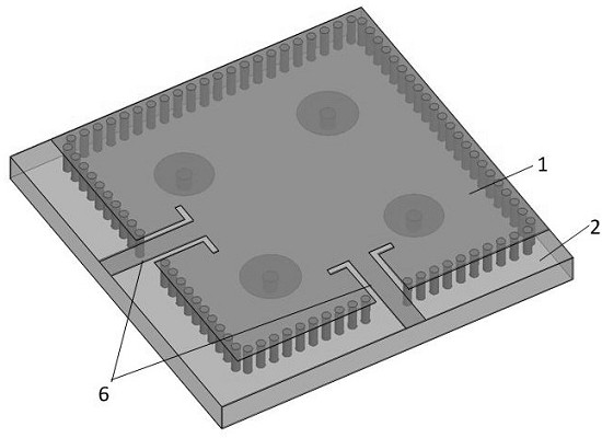
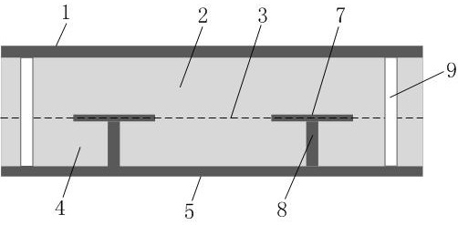
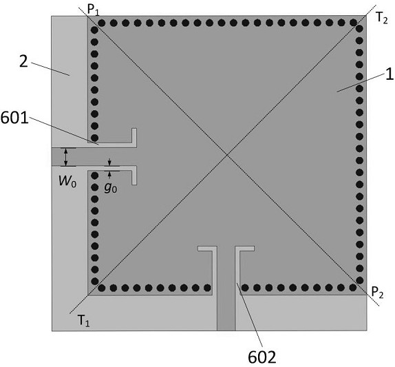
[0026] Such as Figure 1-4 As shown, a capacitive patch-loaded dual-mode substrate integrated waveguide bandpass filter includes a first layer of metal plate 1, a first layer of dielectric plate 2, and a second layer of metal plate 3 arranged in sequence from top to bottom , the second layer of dielectric plate 4 and the third layer of metal plate 5, and fixedly connected in turn, the thickness of the first layer of metal plate 1 and the third layer of metal plate 5 is 30 μm, the first layer of dielectric plate 2 and The model of the second layer of dielectric board 4 is Rogers5880, the thickness is 0.25mm, and the relative dielectric constant is 2.2. The surface of the first layer of metal plate 1 is provided with a microstrip to coplanar waveguide feeder structure 6, so The second layer metal plate 3 includes four capacitive patches 7, the third layer metal plate 5 is fully metal-covered ground, and the second layer dielectric plate 4 is provided with a metallized blind hole...
Embodiment 2
[0034] Such as Figure 1-4 As shown, a capacitive patch-loaded dual-mode substrate integrated waveguide bandpass filter includes a first layer of metal plate 1, a first layer of dielectric plate 2, and a second layer of metal plate 3 arranged in sequence from top to bottom , the second layer of dielectric plate 4 and the third layer of metal plate 5, and fixedly connected in turn, the thickness of the first layer of metal plate 1 and the third layer of metal plate 5 is 40 μm, the first layer of dielectric plate 2 and The model of the second layer of dielectric board 4 is Rogers5880, the thickness is 0.26mm, and the relative dielectric constant is 2.2. The surface of the first layer of metal plate 1 is provided with a microstrip to coplanar waveguide feeder structure 6, so The second layer metal plate 3 includes four capacitive patches 7, the third layer metal plate 5 is fully metal-covered ground, and the second layer dielectric plate 4 is provided with a metallized blind hole...
Embodiment 3
[0042] Such as Figure 1-4 As shown, a capacitive patch-loaded dual-mode substrate integrated waveguide bandpass filter includes a first layer of metal plate 1, a first layer of dielectric plate 2, and a second layer of metal plate 3 arranged in sequence from top to bottom , the second layer of dielectric plate 4 and the third layer of metal plate 5, and fixedly connected in turn, the thickness of the first layer of metal plate 1 and the third layer of metal plate 5 is 35 μm, the first layer of dielectric plate 2 and The model of the second layer of dielectric board 4 is Rogers5880, the thickness is 0.254mm, and the relative dielectric constant is 2.2. The surface of the first layer of metal plate 1 is provided with a microstrip to coplanar waveguide feeder structure 6, so The second layer metal plate 3 includes four capacitive patches 7, the third layer metal plate 5 is fully metal-covered ground, and the second layer dielectric plate 4 is provided with a metallized blind hol...
PUM
| Property | Measurement | Unit |
|---|---|---|
| thickness | aaaaa | aaaaa |
| diameter | aaaaa | aaaaa |
| width | aaaaa | aaaaa |
Abstract
Description
Claims
Application Information
 - Generate Ideas
- Intellectual Property
- Life Sciences
- Materials
- Tech Scout
- Unparalleled Data Quality
- Higher Quality Content
- 60% Fewer Hallucinations
Browse by: Latest US Patents, China's latest patents, Technical Efficacy Thesaurus, Application Domain, Technology Topic, Popular Technical Reports.
© 2025 PatSnap. All rights reserved.Legal|Privacy policy|Modern Slavery Act Transparency Statement|Sitemap|About US| Contact US: help@patsnap.com