Semitransparent perovskite solar cell, assembly and preparation method
A solar cell and perovskite technology, applied in semiconductor/solid-state device manufacturing, electrical components, semiconductor devices, etc., can solve the problems of unfavorable commercialization and market application, low photoelectric conversion efficiency of solar cells, etc., and achieve enhanced charge transport capacity , Inhibit diffusion and improve performance
- Summary
- Abstract
- Description
- Claims
- Application Information
AI Technical Summary
Problems solved by technology
Method used
Image
Examples
Embodiment 1
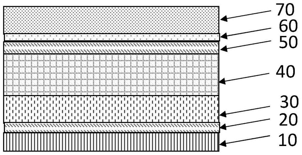
[0039] Embodiment 1 selects the materials of the top charge transport layer in the trans structure as PCBM and TiOx respectively
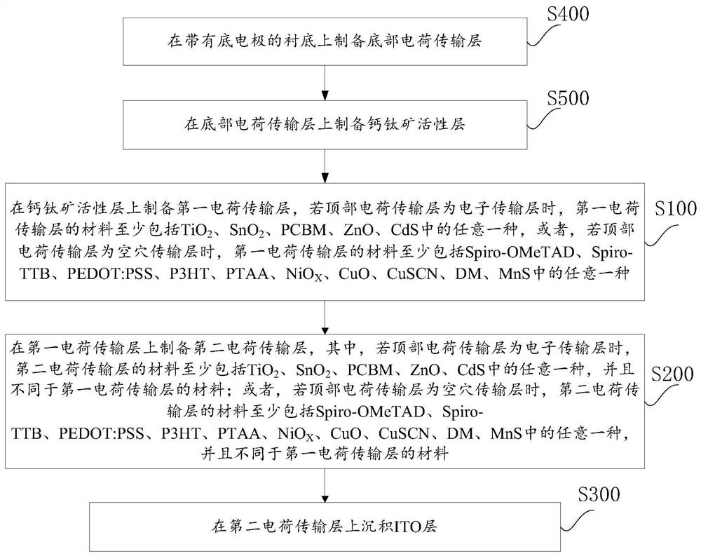
[0040] 1. Use glass / ITO with a thickness of 2mm as the substrate / cathode, perform UV / ozone treatment on the surface, and then spin-coat PTAA solution on the FTO: PTAA is dissolved in chlorobenzene with a concentration of 5mg / ml, and the spin-coating speed is 5000 rpm. After the spin coating is completed, a hole transport layer with a thickness of about 50 nm is obtained;
[0041] 2. Dissolve lead iodide at a concentration of 600mg / ml in a solvent mixed with DMF / DMSO at a ratio of 4:1. After fully heating and stirring to dissolve, the lead iodide solution is filtered through a polytetrafluoroethylene filter membrane with a diameter of 0.45 microns. Spin coating on the hole transport layer in step S1 at a speed of 2000 rpm, and heat at 80° C. for 1 min to obtain a lead iodide layer with a thickness of about 150 nm;
[0042] 3. Continue to spin-coat...
Embodiment 2
[0045] Example 2 selects the material of the top charge transport layer in the trans structure as TiO x and SnO 2
[0046] In this embodiment, except for step 4, other steps are the same as those in embodiment 1, and reference may be made to the description in embodiment 1.
[0047] 4. Add 200uL of SnO 2 The stock solution was diluted with two volumes of absolute ethanol to obtain SnO 2 solution. Take 60uL of SnO 2 solution, set the spin-coating speed to 4000rpm, spin-coating time to 30s, and anneal at 150°C for 20min after spin-coating; mix 70uL of acetylacetonate isopropyl titanate solution with 900uL of methanol and 50uL of concentrated hydrochloric acid solution, and stir continuously to dissolve , configured as a TiOx solution. Take 60uL of TiOx solution, set the spin-coating speed to 5000rpm, spin-coating time to 30s, and anneal at 150°C for 20min after the spin-coating is completed, to obtain a top charge transport layer with a two-layer structure.
Embodiment 3
[0048] Embodiment 3 selects the materials of the top charge transport layer in the trans structure as PCBM and CdS respectively
[0049] In this embodiment, except for step 4, other steps are the same as those in embodiment 1, and reference may be made to the description in embodiment 1.
[0050] 4. In vacuum evaporation equipment, evaporate a 20nm PCBM layer, and then use a magnetron sputtering equipment to sputter 20nm CdS to obtain a top charge transport layer with a two-layer structure.
PUM
| Property | Measurement | Unit |
|---|---|---|
| thickness | aaaaa | aaaaa |
| thickness | aaaaa | aaaaa |
| thickness | aaaaa | aaaaa |
Abstract
Description
Claims
Application Information
 - R&D
- Intellectual Property
- Life Sciences
- Materials
- Tech Scout
- Unparalleled Data Quality
- Higher Quality Content
- 60% Fewer Hallucinations
Browse by: Latest US Patents, China's latest patents, Technical Efficacy Thesaurus, Application Domain, Technology Topic, Popular Technical Reports.
© 2025 PatSnap. All rights reserved.Legal|Privacy policy|Modern Slavery Act Transparency Statement|Sitemap|About US| Contact US: help@patsnap.com


