A lattice-mismatched triple-junction gallium arsenide solar cell and its manufacturing method
A technology of lattice mismatch and solar cells, which is applied in the field of solar cells, can solve problems such as incomplete stress release, many production steps, and reduced performance of mid-bottom tunneling junctions, so as to achieve the effects of reducing damage and shortening the production cycle of products
- Summary
- Abstract
- Description
- Claims
- Application Information
AI Technical Summary
Problems solved by technology
Method used
Image
Examples
Embodiment 1
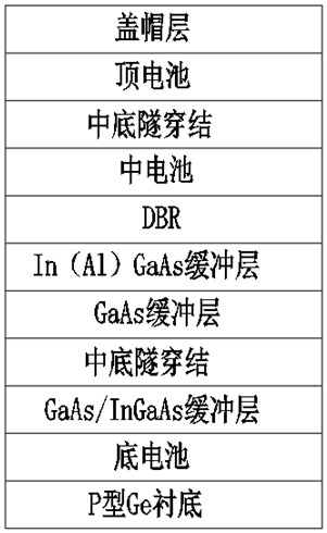
[0036] S1: On a P-type Ge substrate, at 720°C, by pH 3 In the form of diffusion, the emitter area of the bottom cell is formed. The thickness of the emitter area is 0.1 μm, and then the temperature is lowered to 640 ° C to grow a GaInP nucleation layer with a thickness of 0.01 μm. The nucleation layer also serves as the window layer of the bottom cell;
[0037] S2: Increase the temperature to 650°C to grow GaAs / In 0.01 GaAs buffer layer, GaAs thickness is 0.1μm, In 0.01 GaAs thickness is 0.1μm;
[0038] S3: The temperature is lowered to 560°C, and the mid-bottom tunneling junction is grown, and the mid-bottom tunneling junction is N ++ GaAs / P ++ GaAs structure, where N ++ GaAs has a thickness of 0.01 μm and a doping concentration of 1×10 19 / cm 3 , the dopant is a combination of Te and Si; P ++ The thickness of GaAs is 0.01 μm, and the doping concentration is 2×10 19 / cm 3 , the dopant is C;
[0039] S4: The temperature is increased to 650°C, and a GaAs buffer layer ...
Embodiment 2
[0047] S1: On a P-type Ge substrate, at 720°C, by pH 3 In the form of diffusion, the emitter area of the bottom cell is formed. The thickness of the emitter area is 0.3 μm, and then the temperature is lowered to 640 ° C to grow an AlGaInP nucleation layer with a thickness of 0.02 μm. The nucleation layer also serves as the window layer of the bottom cell;
[0048] S2: Increase the temperature to 650°C to grow GaAs / In 0.01 GaAs buffer layer, GaAs thickness is 0.1μm, In 0.01 GaAs thickness is 0.4μm;
[0049] S3: The temperature is lowered to 560°C, and the mid-bottom tunneling junction is grown, and the mid-bottom tunneling junction is N ++ GaAs / P ++ GaAs structure, where N ++ GaAs has a thickness of 0.02 μm and a doping concentration of 3×10 19 / cm 3 , the dopant is a combination of Te and Se; P ++ The thickness of GaAs is 0.02 μm, and the doping concentration is 5×10 19 / cm 3 , the dopant is Zn;
[0050] S4: The temperature is increased to 650°C, and a GaAs buffer ...
Embodiment 3
[0058] S1: On a P-type Ge substrate, at 720°C, by pH 3 In the form of diffusion, the emitter area of the bottom cell is formed. The thickness of the emitter area is 0.4 μm, and then the temperature is lowered to 640 ° C to grow a GaInP nucleation layer with a thickness of 0.03 μm. The nucleation layer also serves as the window layer of the bottom cell;
[0059] S2: Increase the temperature to 650°C to grow GaAs / In 0.01 GaAs buffer layer, GaAs thickness is 0.8μm, In 0.01 GaAs thickness is 0.8μm;
[0060] S3: The temperature is lowered to 560°C, and the mid-bottom tunneling junction is grown, and the mid-bottom tunneling junction is N ++ GaAs / P ++ GaAs structure, where N ++ The thickness of GaAs is 0.03μm, and the doping concentration is 5×10 19 / cm 3 , the dopant is a combination of Se and Si; P ++ GaAs has a thickness of 0.03 μm and a doping concentration of 1×10 20 / cm 3 , the dopant is Mg;
[0061] S4: The temperature is increased to 650°C, and a GaAs buffer laye...
PUM
| Property | Measurement | Unit |
|---|---|---|
| thickness | aaaaa | aaaaa |
| thickness | aaaaa | aaaaa |
| thickness | aaaaa | aaaaa |
Abstract
Description
Claims
Application Information
 - Generate Ideas
- Intellectual Property
- Life Sciences
- Materials
- Tech Scout
- Unparalleled Data Quality
- Higher Quality Content
- 60% Fewer Hallucinations
Browse by: Latest US Patents, China's latest patents, Technical Efficacy Thesaurus, Application Domain, Technology Topic, Popular Technical Reports.
© 2025 PatSnap. All rights reserved.Legal|Privacy policy|Modern Slavery Act Transparency Statement|Sitemap|About US| Contact US: help@patsnap.com


