Eureka AIR delivers breakthrough ideas for toughest innovation challenges, trusted by R&D personnel around the world.

Overlay deviation value correction method, electronic equipment and computer readable storage medium

A technology of overlay deviation and threshold value, applied in microlithography exposure equipment, optomechanical equipment, complex mathematical operations, etc. Improve data accuracy, simple and accurate calculation, and improve the effect of overlay correction accuracy

Active Publication Date: 2020-12-01
INST OF MICROELECTRONICS CHINESE ACAD OF SCI +1
View PDF5 Cites 4 Cited by
  • Summary
  • Abstract
  • Description
  • Claims
  • Application Information

AI Technical Summary

Problems solved by technology

[0004]The processing process of the prior art generally ignores the influence of the measurement error, so the measurement error will not be calculated; or when calculating the measurement error, a batch of wafer groups need to be used At least 3 wafers in and calculate the overlay deviation, the operation is complicated and the accuracy is not high
However, this method of obtaining overlay measurement error often does not reflect the measurement error of a single wafer or certain area overlay marks
In particular, for complex three-dimensional stacked structures or wafers after heat treatment, the overlay correction algorithm often uses the field-by-field exposure method (CPE), which generally can only overlay one wafer in a batch of wafer groups. If the wafer has random process fluctuations or measurement fluctuations, it is not only difficult to find the problem based on the existing technology, but also the problem of overcorrection will occur

Method used


Image

  • Overlay deviation value correction method, electronic equipment and computer readable storage medium
  • Overlay deviation value correction method, electronic equipment and computer readable storage medium
  • Overlay deviation value correction method, electronic equipment and computer readable storage medium

Examples


Embodiment Construction

[0042] In order to make the purpose, technical solution and advantages of the present application clearer, the present application will be further described below in conjunction with the accompanying drawings and specific embodiments. It should be understood that the specific embodiments described here are only used to explain the present application, not to limit the present application. Based on the embodiments in this application, all other embodiments obtained by persons of ordinary skill in the art without making creative efforts belong to the scope of protection of this application.

[0043] Those skilled in the art can understand that, unless otherwise defined, all terms (including technical terms and scientific terms) used herein have the same meanings as commonly understood by those of ordinary skill in the art to which this application belongs. It should also be understood that terms, such as those defined in commonly used dictionaries, should be understood to have m...


PUM


Abstract

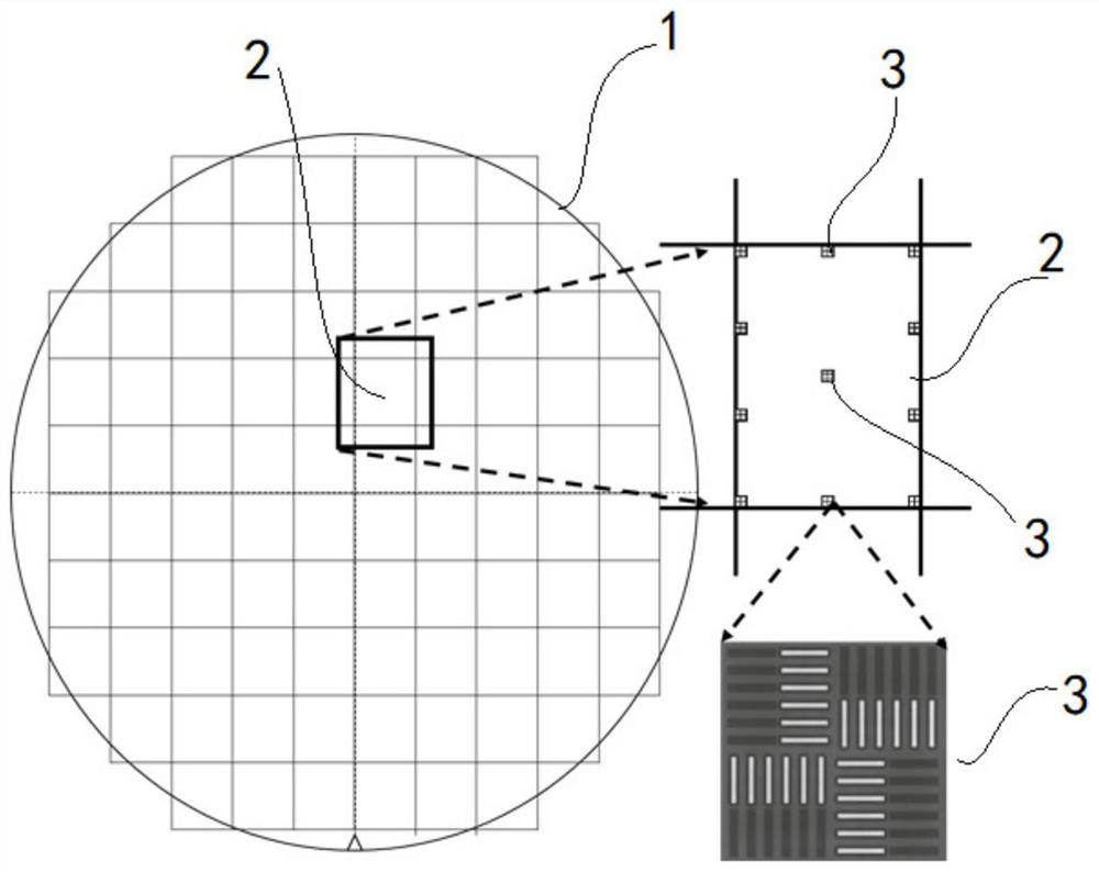
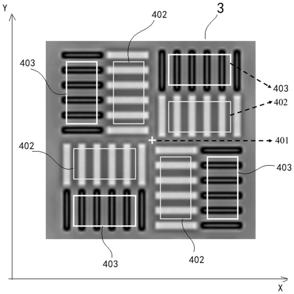
The invention discloses an overlay deviation value correction method, electronic equipment and a computer readable storage medium. The method comprises the following steps of providing a wafer comprising a plurality of exposure areas, selecting a plurality of exposure areas, and determining a plurality of to-be-detected overlay identifiers from the selected exposure areas, calculating the image ofeach to-be-detected overlay identifier for multiple times to obtain a plurality of overlay deviation measurement values, calculating an average value and a standard deviation of the overlay deviationmeasurement value, and taking the average value and the standard deviation as an overlay deviation value and a measurement error value respectively, setting a weight in negative correlation with eachmeasurement error value according to the measurement error value, and performing weighted assignment correction on each overlay deviation value by utilizing each measurement error value and the set weight. According to the method, the average value and the standard deviation of the overlay deviation measurement value serve as the overlay deviation value and the measurement error value respectively, the overlay deviation is corrected based on the measurement error value, the influence of the measurement error is fully considered when the overlay correction parameter is calculated, and the overlay correction accuracy is improved.

Description

technical field [0001] The present application relates to the technical field of semiconductor manufacturing, and in particular to a method for correcting an overlay deviation value, electronic equipment, and a computer-readable storage medium. Background technique [0002] Overlay correction technology is very important for integrated circuits, especially as the process node continues to decrease, the core size continues to shrink, and the overlay deviation value is required to continue to shrink, but the process and measurement effects will not decrease proportionally with the node shrinkage, making It occupies an increasing proportion in overlay correction technology. [0003] The basic method of the existing overlay correction technology is: obtain the wafer with the reference layer and the current layer, measure the overlay error on the overlay measuring machine, and directly correct the overlay error of the wafer. When measuring the overlay value of a wafer, the error...

Claims


Application Information

Patent Timeline
IPC IPC(8): G03F7/20G06F17/10
CPCG03F7/70633G03F7/70516G06F17/10
Inventor 张利斌韦亚一冯耀斌陆聪
Owner INST OF MICROELECTRONICS CHINESE ACAD OF SCI
Why Eureka
Eureka Blog
Learn More