Glass with low resistance and low optical loss and preparation method thereof
An optical loss, low resistance technology, applied in ion implantation plating, coating, metal material coating process, etc., can solve problems such as difficult to meet comprehensive use performance, conflict between optical performance and electrical performance of thin film materials, etc., to reduce optical performance. Loss, not easy to be corroded and oxidized, and the effect of reducing resistance
- Summary
- Abstract
- Description
- Claims
- Application Information
AI Technical Summary
Problems solved by technology
Method used
Image
Examples
Embodiment 1
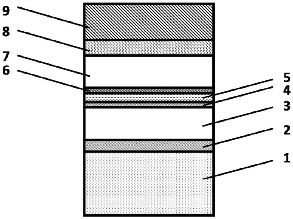
[0042] Glass with low resistance and low optical loss: A transition layer, a first dielectric layer, a first protective layer, a conductive layer, a second protective layer, and a Second medium layer, anti-reflection layer, wear-resistant layer. The first and second dielectric layers are AZO, the first and second protective layers are NiCr, the conductive layer is Au, and the antireflection layer is Nb 2 o 5 , the wear layer is C 3 N 4 . The glass with low electrical resistance and low optical loss, the steps of its preparation method are,
[0043] (1) Use isopropanol and petroleum ether to clean the surface of the tempered glass.
[0044](2) Using plasma to perform surface pretreatment and activation on the cleaned strengthened glass.
[0045] (3) Coating 15nm SiO on the surface of the pretreated strengthened glass by DC pulse magnetron sputtering technology 2 The thin film acts as a transition layer.
[0046] (1) AZO film of 50nm is plated on the transition layer by ...
Embodiment 2
[0057] Glass with low resistance and low optical loss: A transition layer, a first dielectric layer, a first protective layer, a conductive layer, a second protective layer, and a Second medium layer, anti-reflection layer, wear-resistant layer. The first and second dielectric layers are AZO films, the first and second protective layers are NiCr, the conductive layer is Au, and the antireflection layer is SiO 2 , the wear layer is Si 3 N 4 . The glass with low electrical resistance and low optical loss, the steps of its preparation method are,
[0058] (1) Use isopropanol and petroleum ether to clean the surface of the tempered glass.
[0059] (2) Using plasma to perform surface pretreatment and activation on the cleaned strengthened glass.
[0060] (3) Coating 18nm SiO on the surface of the pretreated strengthened glass by DC pulse magnetron sputtering technology 2 The thin film acts as a transition layer.
[0061] (4) AZO film of 60nm is plated on the transition layer...
Embodiment 3
[0072] Glass with low resistance and low optical loss: coating transition layer, plated first dielectric layer, first protective layer, conductive layer, second protective layer, second dielectric layer on polymethyl methacrylate with a thickness of 10mm layer, anti-reflective layer, wear-resistant layer. The first and second dielectric layers are AZO films, the first and second protective layers are NiCr, the conductive layer is Au, and the antireflection layer is SiO 2 , the wear layer is C 3 N 4 . The glass with low electrical resistance and low optical loss, the steps of its preparation method are,
[0073] (1) Use isopropanol and petroleum ether to clean the surface of reinforced glass polymethyl methacrylate.
[0074] (2) Using plasma to pretreat and activate the surface of the cleaned polymethyl methacrylate.
[0075] (3) Coating a layer of acrylic and polyurethane mixture on the pretreated polymethyl methacrylate surface by coating technology and curing it as a tr...
PUM
| Property | Measurement | Unit |
|---|---|---|
| thickness | aaaaa | aaaaa |
| thickness | aaaaa | aaaaa |
| thickness | aaaaa | aaaaa |
Abstract
Description
Claims
Application Information
 - R&D
- Intellectual Property
- Life Sciences
- Materials
- Tech Scout
- Unparalleled Data Quality
- Higher Quality Content
- 60% Fewer Hallucinations
Browse by: Latest US Patents, China's latest patents, Technical Efficacy Thesaurus, Application Domain, Technology Topic, Popular Technical Reports.
© 2025 PatSnap. All rights reserved.Legal|Privacy policy|Modern Slavery Act Transparency Statement|Sitemap|About US| Contact US: help@patsnap.com

