
Processing device for semiconductor graphite wafer and processing method thereof

A processing device and semiconductor technology, applied in the direction of fine working device, stone processing equipment, semiconductor/solid-state device manufacturing, etc., can solve the problems of increasing operator workload, large wafer cutting error, and reducing product productivity, etc. Improve the success rate, facilitate cutting, and improve work efficiency

Inactive Publication Date: 2020-11-24
DATONG XINCHENG NEW MATERIAL CO LTD
View PDF7 Cites 0 Cited by
  • Summary
  • Abstract
  • Description
  • Claims
  • Application Information

AI Technical Summary

Problems solved by technology

However, when the existing wafer cutting equipment is in use, the positions of the workbench and the cutter are fixed. When the cut wafer needs to change the direction of cutting, the wafer needs to be removed and fixed in the slot. In this way, the workload of the operator is increased and the work efficiency is reduced; when the wafer is removed, the error of wafer cutting is large, which leads to the failure of crystal cutting and reduces the productivity of the product

Method used


Image

  • Processing device for semiconductor graphite wafer and processing method thereof
  • Processing device for semiconductor graphite wafer and processing method thereof
  • Processing device for semiconductor graphite wafer and processing method thereof

Examples


Embodiment 1

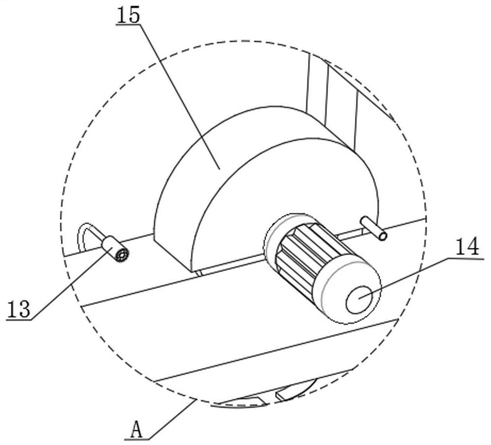
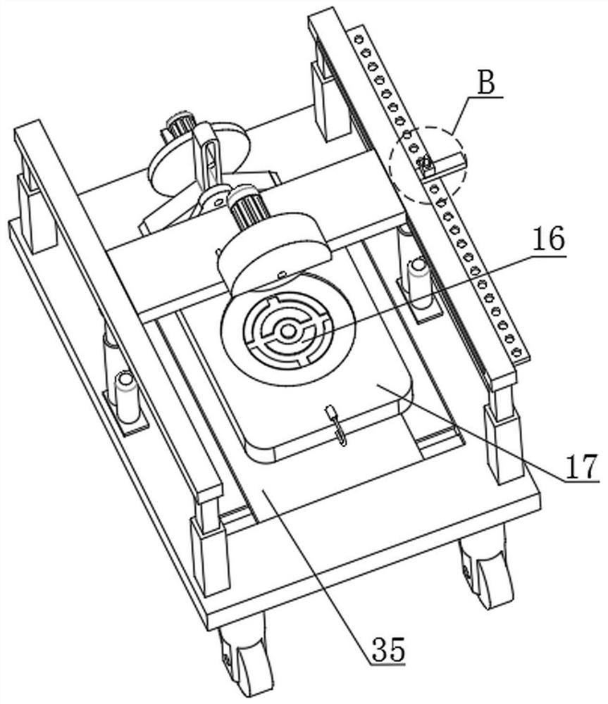
[0033] Embodiment 1: see Figure 1-8 , a processing device for semiconductor graphite wafers, including a base 1, the base 1 is a rectangular plate placed horizontally, a rectangular groove is opened in the middle of the top surface of the base 1, and the bottom surface of the rectangular groove is symmetrical at both ends longitudinally A first T-shaped slot is provided, and a first T-shaped slider is slidably connected in each of the first T-shaped slots, and the top surface of each first T-shaped slider is fixed on the movable plate 35. On the bottom surface, it is convenient for the movable plate 35 to slide in the rectangular groove; the top side edge of the movable plate 35 is provided with an adjustment assembly, which is convenient to adjust the front and rear movement of the movable plate 35; the middle part of the top surface of the movable plate 35 is provided with The rotating assembly, the top of the fixed shaft 38 in the rotating assembly is affixed with the work...

Embodiment 2

[0040] Embodiment 2: refer to Figure 8 , in the present embodiment, the present invention also proposes the processing method for the processing device of semiconductor graphite wafer, comprises the following steps:

[0041] Step 1, the first motor 22, the second motor 28, the third motor 14, and the fan are respectively electrically connected to the external power supply through wires, and the water guide pipe is connected to the external water source, and then the circular wafer is put into the card slot, and the negative pressure Groove 16 fixes the circular wafer;

[0042] Step 2, by controlling the first electric push rod 2 and the second electric push rod 9 to drive the second support rod 4 and the fourth support rod 10 to move up and down respectively, the second support rod 4 and the fourth support rod 10 drive the support plate 8 up and down Movement, the support plate 8 drives the cutting assembly to move up and down, and then pushes the support plate 8 to move the...


PUM


Abstract

The invention discloses a processing device for a semiconductor graphite wafer and a processing method of the processing device for the semiconductor graphite wafer. The processing device for the semiconductor graphite wafer comprises a base. The top surface of each first T-shaped sliding block is fixedly connected to the bottom surface of a moving plate. An adjusting assembly is arranged on the edge of one side of the top surface of the moving plate, a rotating assembly is arranged in the middle of the top surface of the moving plate, and a workbench is fixedly connected with the top of a fixing shaft in the rotating assembly. A clamping groove is formed in the middle of the top surface of the workbench, and a negative pressure groove is axially formed in the middle of the top surface ofthe clamping groove. A cutting assembly is fixedly connected to the middle of the top of a supporting plate, a water guide pipe penetrates through one side of a cutter cover in the cutting assembly, one end of a water outlet pipe is arranged in the middle of the water guide pipe, and the other end of the water outlet pipe is located on one side face of a cutter. According to the processing devicefor the semiconductor graphite wafer, the workbench can be moved forwards and backwards through an adjusting device, the workbench can be rotated through a rotating device, and therefore the wafer canbe cut in different directions, the working efficiency is improved, and the cutting error is avoided. Meanwhile, the cutter can ascend and descend, and therefore the wafer is conveniently cut.

Description

technical field [0001] The invention relates to the technical field of wafer processing, in particular to a processing device and a processing method for semiconductor graphite wafers. Background technique [0002] Wafers are dissolved from high-purity polysilicon, mixed with silicon crystal seeds, and then slowly pulled out to form cylindrical single crystal silicon, which is formed after grinding, polishing and slicing silicon crystal rods. At present, wafers are mainly used to make chips. In chip production, whether it is now or based on future development trends, wafer cutting is an extremely important and indispensable process. However, when the existing wafer cutting equipment is in use, the positions of the workbench and the cutter are fixed. When the cut wafer needs to change the direction of cutting, the wafer needs to be removed and fixed in the slot. In this way, the workload of the operator is increased and the work efficiency is reduced; when the wafer is remov...

Claims


Application Information

Patent Timeline
Patent Type & Authority Applications(China)
IPC IPC(8): B28D5/02B28D7/04B28D7/02B28D7/00H01L21/67
CPCB28D5/0058B28D5/0064B28D5/0076B28D5/0088B28D5/023B28D5/024H01L21/67092
Inventor 柴利春张培林武建军张作文王志辉
Owner DATONG XINCHENG NEW MATERIAL CO LTD
Learn More