Alignment pattern, semiconductor structure with alignment pattern and manufacturing method of semiconductor structure

A technology for aligning patterns and manufacturing methods, which is applied in semiconductor/solid-state device manufacturing, semiconductor devices, and photoengraving processes of patterned surfaces. It can solve problems such as poor quasi-quality and achieve area reduction, area reduction, and elimination The effect of the etch loading effect

Pending Publication Date: 2020-11-20
CHANGXIN MEMORY TECH INC
View PDF0 Cites 1 Cited by
  • Summary
  • Abstract
  • Description
  • Claims
  • Application Information

AI Technical Summary

Problems solved by technology

[0005] The purpose of the present invention is to provide an alignment pattern, a semiconductor structure with an alignment pattern and a manufacturing method thereof, so as to solve the problem of poor alignment quality

Method used


Image

  • Alignment pattern, semiconductor structure with alignment pattern and manufacturing method of semiconductor structure
  • Alignment pattern, semiconductor structure with alignment pattern and manufacturing method of semiconductor structure
  • Alignment pattern, semiconductor structure with alignment pattern and manufacturing method of semiconductor structure

Examples


Embodiment Construction

[0027] It can be seen from the background art that the accuracy of alignment using existing alignment patterns needs to be improved.

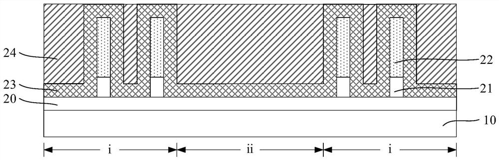
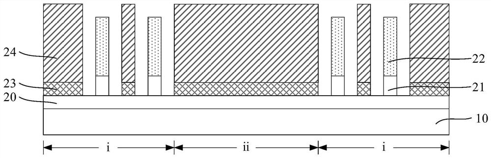
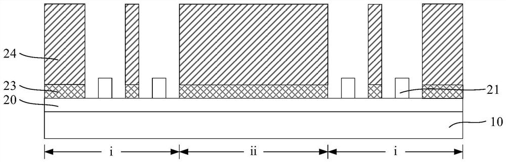
[0028] Figure 1 to Figure 4 It is a structural schematic diagram corresponding to each step of a method for forming a semiconductor structure with aligned patterns.

[0029] refer to figure 1 , providing a substrate comprising a first region i and a second region ii located between adjacent first regions i, the substrate comprising a substrate 10 and a polysilicon layer 20 located on the surface of the substrate 10, the surface of the substrate of the first region i is formed with discrete The first dielectric layer 21 has a photoresist layer 22 on the top surface of the first dielectric layer 21; a second dielectric layer 23 is also formed on the surface of the base, and the second dielectric layer 23 also covers the top and sidewalls of the photoresist layer 22. The thickness of the second dielectric layer 23 is smaller than that of the fi...


PUM


Abstract

The invention relates to an alignment pattern, a semiconductor structure with the alignment pattern, and a manufacturing method of the semiconductor structure. The manufacturing method comprises the following steps of: arranging at least two standard pattern areas along a first direction, wherein each standard pattern area comprises at least two discrete sub-pattern areas, in the first direction,the distance between the adjacent sub-pattern areas in each standard pattern area is a first distance, the distance between the adjacent standard pattern areas is a second distance, and the second distance is larger than the first distance; and arranging shielding patterns, wherein the shielding patterns are located between the adjacent standard pattern areas, and gaps are formed between the shielding patterns and the adjacent standard pattern areas. According to the invention, the area of the open area in the alignment pattern can be reduced, and the defect problem caused by etching residuesis avoided, so that the alignment quality is improved.

Description

technical field [0001] The invention relates to the technical field of semiconductors, in particular to an alignment pattern, a semiconductor structure with the alignment pattern and a manufacturing method thereof. Background technique [0002] Alignment is one of the most critical influencing factors in the semiconductor manufacturing process. For example, in lithography technology, it is necessary to pay attention to the alignment between the exposure machine and the mask plate, and in the chip scribing process, it is necessary to pay attention to the actual scribing area and the scribing area. Alignment between slots. [0003] Taking alignment in lithography technology as an example, there are mainly the following types of alignment methods commonly used in lithography technology: alignment based on bright and dark fields, grating diffraction alignment, and video image alignment. In order to achieve alignment, it is necessary to set a corresponding alignment pattern (Ali...

Claims


Application Information

Patent Timeline
IPC IPC(8): H01L23/544H01L21/027H01L21/033G03F1/42
CPCG03F1/42H01L21/0274H01L21/0332H01L23/544H01L2223/54426
Inventor 范聪聪
Owner CHANGXIN MEMORY TECH INC
Why Eureka
Try Eureka