Electro-optic crystal film, preparation method thereof and electro-optic modulator
A technology of electro-optic crystals and thin films, applied in light guides, optics, instruments, etc., can solve the problems of large optical transmission loss, achieve the effects of reducing diffuse reflection, simple process, and ensuring uniformity and integrity
- Summary
- Abstract
- Description
- Claims
- Application Information
AI Technical Summary
Problems solved by technology
Method used
Image
Examples
preparation example Construction
[0060] Specifically, such as Figure 5 Shown, described preparation method comprises the following steps:
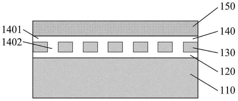
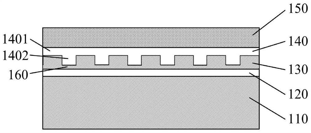
[0061] Step 1. Prepare a silicon-on-insulator structure, and etch the top silicon layer of the silicon-on-insulator structure to form a silicon waveguide layer; wherein, the silicon-on-insulator structure is a silicon substrate layer, a silicon dioxide layer, and a silicon dioxide layer from bottom to top. Top layer silicon; groove structure formed in the silicon waveguide layer after etching.
[0062] In this application, the silicon-on-insulator structure is also called SOI wafer, and an SOI wafer structure with a size of 4 inches can be selected. The SOI wafer structure is: 50nm-50μmSi / 50nm-5μmSiO from top to bottom 2 / Si, the top layer of silicon is etched by dry etching, and the top layer of silicon is etched into a ridge strip waveguide; wherein, the top layer of silicon is completely etched or partially etched.
[0063] If complete etching is used, the processed...
Embodiment 1
[0079] (1) Prepare an SOI wafer with a size of 4 inches, a thickness of 0.5mm and a smooth surface. The SOI wafer structure is 220nmSi / 2μmSiO from top to bottom 2 / Si. The top layer silicon of the SOI wafer is etched by dry etching, the top layer SI is completely etched, and a ridge-shaped strip waveguide is etched out. The size of the ridge-shaped strip waveguide is 1 μm in width*220 nm in thickness. After etching A groove structure is formed in the silicon waveguide layer, and the height of the groove structure is the thickness of the ridge strip waveguide.
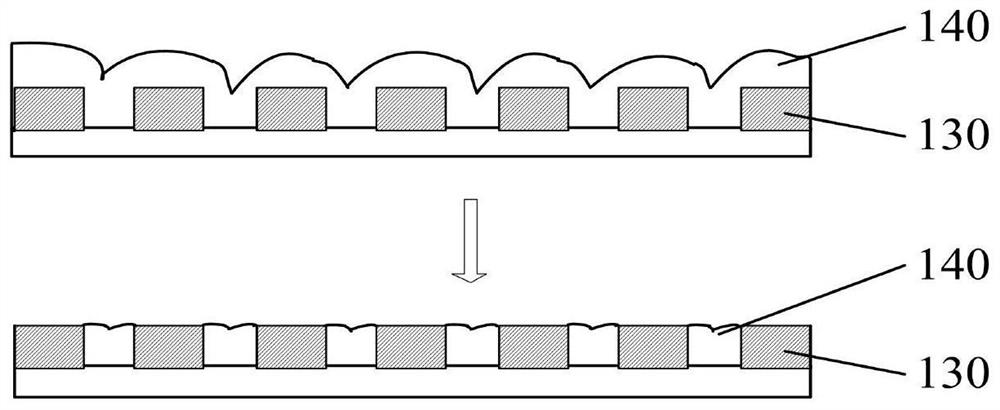
[0080] (2) Clean the ridge-shaped strip waveguide surface of the SOI wafer after etching, and deposit a layer of 2.5 μm SiO on the ridge-shaped silicon waveguide surface by PECVD 2 , filling the groove structure and covering the silicon waveguide layer to form a cladding isolation layer.
[0081] (3) For the SiO covered ridge waveguide in step (2) 2 Use CMP process to planarize, repeat PECVD to deposit silicon dioxi...
Embodiment 2
[0088] (1) Prepare an SOI wafer with a size of 4 inches, a thickness of 0.5mm and a smooth surface. The SOI wafer structure is 220nmSi / 2μmSiO from top to bottom 2 / Si. The top layer Si of the SOI wafer is etched by dry etching, the top layer Si is completely etched, and a ridge-shaped strip waveguide is etched out. The size of the ridge-shaped strip waveguide is 1 μm in width*220 nm in thickness. After etching A groove structure is formed in the silicon-based groove waveguide layer, and the height of the groove structure is the thickness of the ridge waveguide.
[0089] (2) Clean the ridge-shaped strip waveguide surface of the SOI wafer after etching, and deposit a layer of 2.5 μm SiO on the ridge-shaped silicon waveguide surface by PECVD 2 , filling the groove structure and covering the silicon waveguide layer to form a cladding isolation layer.
[0090] (3) For the SiO covered ridge silicon waveguide in step (2) 2 Use CMP process to planarize, repeat PECVD to deposit sil...
PUM
| Property | Measurement | Unit |
|---|---|---|
| Thickness | aaaaa | aaaaa |
| Flatness | aaaaa | aaaaa |
| Roughness | aaaaa | aaaaa |
Abstract
Description
Claims
Application Information
 - R&D
- Intellectual Property
- Life Sciences
- Materials
- Tech Scout
- Unparalleled Data Quality
- Higher Quality Content
- 60% Fewer Hallucinations
Browse by: Latest US Patents, China's latest patents, Technical Efficacy Thesaurus, Application Domain, Technology Topic, Popular Technical Reports.
© 2025 PatSnap. All rights reserved.Legal|Privacy policy|Modern Slavery Act Transparency Statement|Sitemap|About US| Contact US: help@patsnap.com


