Dynamic frequency selective surface structure and preparation method thereof
A frequency selective surface and dynamic frequency selection technology, applied in the electromagnetic field, can solve problems such as the deterioration of the performance of integrated circuit components
- Summary
- Abstract
- Description
- Claims
- Application Information
AI Technical Summary
Problems solved by technology
Method used
Image
Examples
example 1
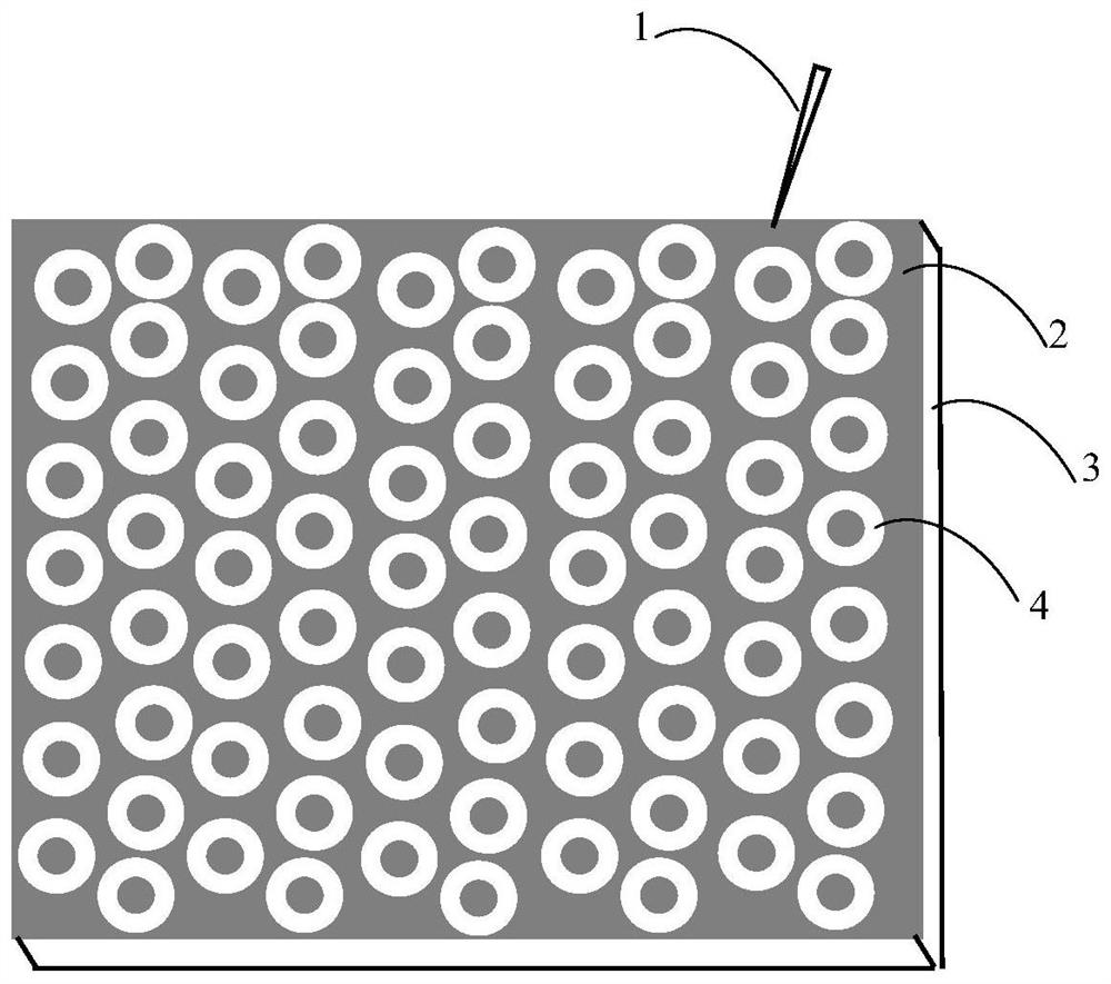
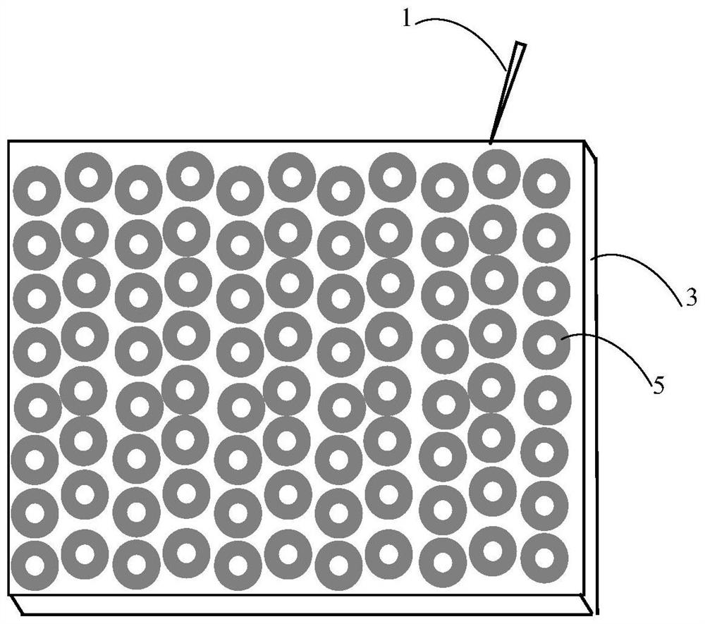
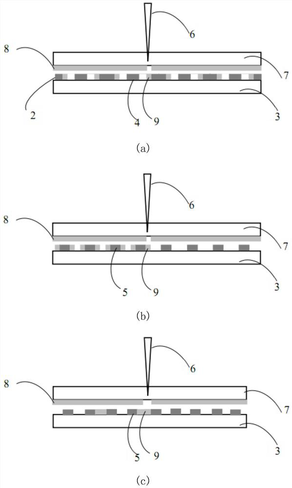
[0059] Select a dielectric substrate F4B-2 sample with a size of 500mm×500mm, a thickness of 0.5mm, a relative permittivity ε=2.65, and a 0.03mm thick copper film on the surface, and use laser selective etching technology on the sample. Selectively remove the copper film material to prepare a ring-shaped unit structure with gaps arranged in a radius of 2.3mm, an inner radius of 1.9mm, and a period (that is, the distance from the center of adjacent units to the center) of 5mm to form a A band-pass FSS periodic array with fixed resonant frequency. Then, laser-induced forward transfer (LIFT) was used to deposit the undoped ion VO on the lower surface of the glass substrate. 2 The thin film is transferred to the outer wall of the inner ring of the gap ring unit structure with high precision, and is in close contact with the copper film of the inner ring, VO 2 The width of the film is 0.2mm, the thickness is 0.03mm, and it is prepared into a composite unit structure. When the amb...
example 2
[0061] Select a dielectric substrate F4B-2 sample with a size of 500mm×500mm, a thickness of 0.5mm, a relative permittivity ε=2.65, and a 0.03mm thick copper film on the surface, and use laser selective etching technology on the sample. Selectively remove the copper film material to prepare a ring-shaped unit structure of copper sheets with an outer ring radius of 2.3mm, an inner ring radius of 1.9mm, and a period of 5mm to form a band-stop FSS periodic array with a fixed resonant frequency . Then, laser-induced forward transfer (LIFT) was used to deposit the undoped ion VO on the lower surface of the glass substrate. 2 The thin film is transferred to the outer wall of the inner ring of the copper ring unit structure with high precision, and is in close contact with the inner ring copper film, VO 2 The width of the film is 0.3mm, the thickness is 0.03mm, and it is prepared into a composite unit structure. When the ambient temperature is lower than 341K, the FSS reflection re...
example 3
[0063] Select a dielectric substrate F4B-2 sample with a size of 500mm×500mm, a thickness of 0.5mm, a relative permittivity ε=2.65, and a 0.03mm thick copper film on the surface, and use laser selective etching technology on the sample. The copper film material is selectively removed, and a ring-shaped unit structure with an outer ring radius of 2.3 mm, an inner ring radius of 1.9 mm, and a period of 5 mm is prepared to form a band-pass FSS periodic array with a fixed resonance frequency. Then, using laser-induced forward transfer technology (LIFT), the doped 10% Mo ion VO deposited on the lower surface of the glass substrate 2 The thin film (phase transition temperature is 308K) is transferred to the outer wall of the inner ring of the gap ring unit structure with high precision, and is in close contact with the copper film of the inner ring, doped with Mo ions VO 2 The width of the film is 0.1mm, and the thickness is 0.03mm; and then the laser-induced forward transfer techno...
PUM
| Property | Measurement | Unit |
|---|---|---|
| Resonant frequency | aaaaa | aaaaa |
| width | aaaaa | aaaaa |
| thickness | aaaaa | aaaaa |
Abstract
Description
Claims
Application Information
 - R&D Engineer
- R&D Manager
- IP Professional
- Industry Leading Data Capabilities
- Powerful AI technology
- Patent DNA Extraction
Browse by: Latest US Patents, China's latest patents, Technical Efficacy Thesaurus, Application Domain, Technology Topic, Popular Technical Reports.
© 2024 PatSnap. All rights reserved.Legal|Privacy policy|Modern Slavery Act Transparency Statement|Sitemap|About US| Contact US: help@patsnap.com


