Thermal control phase modulator based on sub-wavelength grating metasurface
A technology of phase modulator and sub-wavelength grating, which is applied in the direction of instruments, light guides, optics, etc., can solve the problems of low Q value, insufficient phase mutation, and insufficient sharpness of resonance peak, etc., achieve high Q value, and realize thermal control phase modulation , The effect of high-sensitivity thermal control phase modulation
- Summary
- Abstract
- Description
- Claims
- Application Information
AI Technical Summary
Problems solved by technology
Method used
Image
Examples
Embodiment 1
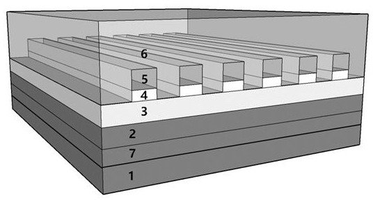
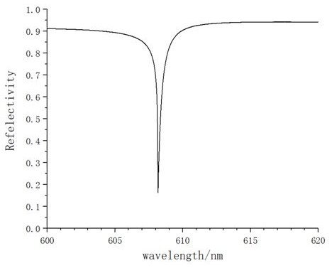
[0025] As shown in Figure 1, the present invention discloses a thermally controlled phase modulator based on a subwavelength grating metasurface, including a six-layer structure of the subwavelength grating metasurface chip, the first layer being the bottom transparent medium substrate 1, The second layer is a metal thin film layer 2, the third layer is a dielectric thin film layer 3, the fourth layer is a dielectric grating layer 4, the fifth layer is a high refractive index dielectric grating layer 5, and the sixth layer is a thermo-optic dielectric layer 6, wherein the heating The electrode array 7 is set between the first layer and the second layer (it can also be set on the sixth layer); by adjusting the parameters of the subwavelength grating metasurface structure, based on the original GMR (Guided-Mode Resonance) resonance peak On the surface, a high-Q resonance peak is derived; the high-Q peak is accompanied by a sharp phase mutation, and the phase mutation curve will d...
Embodiment 2
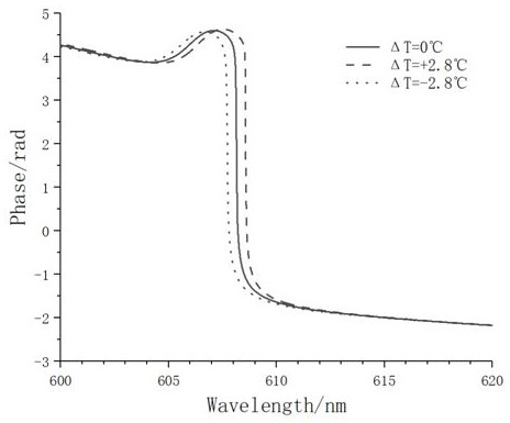
[0027] A thermally controlled phase modulator based on a subwavelength grating metasurface, the material and structural parameters can be selected as follows: the grating period p of the dielectric grating layer 4 and the high refractive index dielectric grating layer 5 are set to 430nm; the grating duty cycle q =0.5; Transparent dielectric substrate 1 chooses SiO 2 ; The metal film layer 2 selects Ag, and the thickness is 150nm; the dielectric film layer 3 selects Si 3 N 4 , the thickness is 160nm; the dielectric grating layer 4 chooses Si 3 N 4 , the thickness t1 is 40nm; the high refractive index dielectric grating layer 5 chooses TiO 2 , the thickness t2 is 280nm, satisfying t14 RIU / °C, when the temperature changes by ±2.8°C, that is, ΔT=±2.8°C, the refractive index of PDMS changes by about 0.001 RIU, that is, Δn=±0.001, so that the change in the refractive index will cause the drift of the phase modulation curve, such as attached image 3 shown. attached image 3 ...
Embodiment 3
[0029] A thermally controlled phase modulator based on a sub-wavelength grating metasurface can adjust the working wavelength accordingly when the grating parameters are changed, and is suitable for phase modulation ranging from visible light to near-infrared bands. attached Figure 4 Shown is the variation curve of the operating wavelength of the thermally controlled phase modulator with the grating parameters. It can be seen that the thermally controlled phase modulator of the subwavelength grating metasurface can work in the visible light band (such as when the grating period p=430nm, the working wavelength is around 608nm) by adjusting the grating parameters, and can also extend the working wavelength to Near-infrared band (for example, when the grating period p=600nm, the working wavelength is around 850nm).
PUM
| Property | Measurement | Unit |
|---|---|---|
| Thickness | aaaaa | aaaaa |
Abstract
Description
Claims
Application Information
 - R&D Engineer
- R&D Manager
- IP Professional
- Industry Leading Data Capabilities
- Powerful AI technology
- Patent DNA Extraction
Browse by: Latest US Patents, China's latest patents, Technical Efficacy Thesaurus, Application Domain, Technology Topic, Popular Technical Reports.
© 2024 PatSnap. All rights reserved.Legal|Privacy policy|Modern Slavery Act Transparency Statement|Sitemap|About US| Contact US: help@patsnap.com


